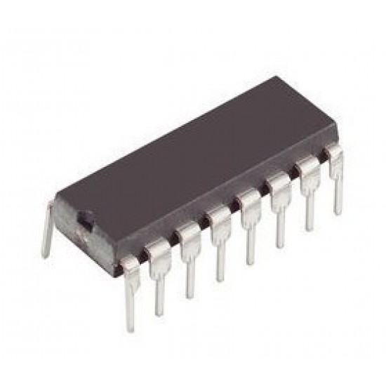
74LS195 Universal 4-Bit Shift Register IC
KES 100.00
- Stock: In Stock
- Model: 74LS195
- SKU: 3662
Your shopping cart is empty!

The SN54/ 74LS195 is a high speed 4-Bit Universal Shift Register offering typical shift frequencies of 39 MHz. It is useful for a wide variety of registers and counting applications. It utilizes the Schottky diode clamped process to achieve high speeds and is fully compatible with all Motorola TTL products. The 74LS195 IC output always comes in TTL which makes it easy to work with other TTL devices and microcontrollers. The IC 74LS195 is smaller in size and it has a much faster speed which makes it reliable in every kind of device.
Universal Shift registers are an integral part of digital memory circuitry usually found in devices such as calculators, computers, and data processing systems. With a universal shift register, data or bits can be entered into the system in a serial or parallel manner. Data entry using 74LS195 is usually done from one direction, and as more data is added, it shifts positions until the data gets to the output end. The two ends are referred to as the left and right ends. Movement of data can be from left to right, from right to left, or in both directions to make a bidirectional shift register.
| Pin No. | Pin Name | Description |
|---|---|---|
| 1 | MR’ | Active Low Master Reset Input |
| 2 | J | First stage J Input |
| 3 | K’ | Active Low First Stage K Input |
| 4 | P0 | Parallel Data Input P0 |
| 5 | P1 | Parallel Data Input P1 |
| 6 | P2 | Parallel Data Input P2 |
| 7 | P3 | Parallel Data Input P3 |
| 8 | GND | Ground Pin |
| 9 | PE’ | Active Low Parallel Enable Input |
| 10 | CP | Clock Pulse Input |
| 11 | Q3′ | Complementary Last Stage Output |
| 12 | Q3 | Parallel Output Q3 |
| 13 | Q2 | Parallel Output Q2 |
| 14 | Q1 | Parallel Output Q1 |
| 15 | Q0 | Parallel Output Q0 |
| 16 | Vcc | Chip Supply Voltage |
