Introduction to Dual Op Amp IC LM358
The LM358 is a highly versatile and widely used dual operational amplifier (op-amp) integrated circuit (IC) that has become a cornerstone in electronics due to its reliability, affordability, and flexibility. This IC integrates two independent, high-gain, frequency-compensated operational amplifiers within a single package, powered by a common power supply. Its design makes it ideal for a broad range of applications, from basic signal amplification to complex analog circuit designs. In this in-depth guide, we will explore the LM358’s features, specifications, pin configuration, operating principles, applications, and advantages, providing a thorough understanding for hobbyists, engineers, and designers.
LM358 Features and Specification
The LM358 is engineered to operate efficiently with a single power supply, supporting a wide voltage range from 3V to 32V, or ±1.5V to ±16V in dual-supply configurations. This flexibility makes it suitable for both low-voltage AC and moderate-voltage DC applications. Its compact packaging, including options like TO-99, CDIP, DSBGA, SOIC, and PDIP, ensures compatibility across various circuit designs and manufacturing processes. The LM358’s ability to handle up to 20 mA per channel, combined with its low power consumption, makes it a go-to choice for cost-sensitive, real-world applications such as transducer amplifiers, DC gain blocks, active filters, and conventional op-amp circuits.
Overview of the LM358 IC
For those familiar with operational amplifiers, the LM358 shares similarities with the classic 741 op-amp but offers the advantage of dual op-amps in a single package and enhanced performance for modern applications. To learn more about the 741 op-amp, you can explore its specifications and applications for a comparative understanding.
Depending upon the manufacturer, each product may have a slightly different variation of the components and each has very similar specifications. Some of these components have identical pinout and package sizes to allow for compatibility between different manufacturers.
Some important features and specifications of LM358 IC are as follows:
Key Features and Specifications
The LM358 is packed with features that make it a robust and adaptable component. While specifications may vary slightly depending on the manufacturer, the core characteristics remain consistent across most versions. Below is a detailed breakdown of its key features and specifications:
Dual Op-Amps in a Single Package: Integrates two independent, internally frequency-compensated operational amplifiers, allowing for simultaneous or independent use in circuit designs.
Wide Power Supply Range:
Single supply: 3V to 32V
Dual supply: ±1.5V to ±16V
High Voltage Gain: Approximately 100 dB, enabling significant signal amplification.
Wide Bandwidth: Unity gain bandwidth of 1 MHz, suitable for a variety of signal processing tasks.
Low Supply Current: Typically 700 µA, making it ideal for battery-powered applications.
High Output Voltage Swing: Provides robust output capabilities for driving loads.
Differential Input Voltage Range: Matches the power supply voltage, enhancing flexibility in input signal handling.
Short-Circuit Protection: Built-in protection for output stages, increasing reliability.
Input Common-Mode Voltage Range: Includes ground, allowing for direct sensing near ground potential.
Operating Temperature Range: 0°C to 70°C, suitable for most standard environments.
Soldering Pin Temperature: Up to 260°C, ensuring compatibility with standard assembly processes.
Available Packages: Includes TO-99, CDIP, DSBGA, SOIC, PDIP, and SOT-25, offering flexibility for different board layouts.
These specifications make the LM358 a reliable choice for both hobbyist projects and professional designs, with its standardized pinout ensuring compatibility across manufacturers.
Pin Configuration
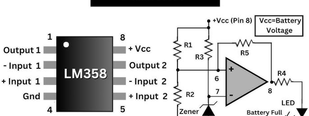
The real image and pinout of the configuration of LM358 IC is shown in the diagram below which has eight pins in total having different individual functions associated with each of them.
- Pin1 and pin8 are the output of the comparator
- Pin2 and pin6 are inverting input.
- Pin3 and pin5 are non-inverting inputs
- Pin4 is the GND terminal
- Pin8 is VCC+/positive supply
All the pins of LM358 IC along with their sequence number are given in the tabular diagram shown below.
LM358 Operating Principle and Working Mechanism
The LM358’s dual op-amps can function as both amplifiers and comparators, depending on the circuit configuration. Below is a detailed explanation of its operation:
Power Supply
Pin 8 (VCC+) is the primary power input. For comparator applications, the LM358 supports a single supply voltage from 3V to 32V. For op-amp applications, it can operate with either a single supply (3V to 32V) or a dual supply (±1.5V to ±16V). This versatility makes it suitable for a wide range of circuit designs.
Op-Amp Operation
Each op-amp (A and B) operates independently:
Op-Amp A: Uses Pin 2 (inverting input) and Pin 3 (non-inverting input), with the output at Pin 1.
Op-Amp B: Uses Pin 6 (inverting input) and Pin 5 (non-inverting input), with the output at Pin 7.
When used as a comparator, the LM358 compares the voltages at the inverting and non-inverting inputs:
If the non-inverting input (Pin 3 for op-amp A, Pin 5 for op-amp B) has a higher voltage than the inverting input (Pin 2 for op-amp A, Pin 6 for op-amp B), the corresponding output (Pin 1 or Pin 7) goes high. If the inverting input voltage exceeds the non-inverting input, the output goes low.
This behaviour makes the LM358 ideal for applications requiring signal comparison or amplification. Notably, the outputs do not require pull-up resistors, simplifying circuit design.
LM358 Applications
LM358 Dual Op-Amp IC is widely used in many real-life applications. Some of the major applications of LM358 IC are listed below:
- DC gain block
- General Signal conditioning
- General Signal Amplification
- Transducer Amplifier
- Operational Amplifier Circuit
- Current Loop Transmitters for 4 to 20 mA
- Active Filters
- Comparators (Loop control & regulation)
- Integrator, Differentiator, Adder, Voltage follower, etc.
- It can be used in real-life applications like shock alarm circuits and dark sensor circuits.
Advantages
The followings are the advantages of LM 358 IC:
- Two operational amplifiers are compensated internally. we can use both op-amps at a time or if we need only one op-amp we can use it
- Two internally compensated for OP-AMP
- Removes the necessity of dual supplies
- Power drains suitable for operation of the battery
- Permits direct sensing close to GND and VOUT
- Compatibility with all forms of logic
LM 358 IC Packages
LM358 Dual Op-Amp IC has four different types of packages and they are DSBGA, PDIP, TO-CAN, and SOT-25(5). All of these packages along with their dimensions and part numbers are given in the tabular diagram shown below.
Conclusion
The LM358 dual operational amplifier IC is a powerful, cost-effective, and versatile component that has earned its place in countless electronic designs. Its ability to operate over a wide voltage range, coupled with its low power consumption and robust feature set, makes it an ideal choice for applications ranging from simple signal amplification to complex analog signal processing. Whether you’re a hobbyist building a sensor circuit or an engineer designing an industrial control system, the LM358 provides the performance and reliability needed to bring your projects to life. For further exploration of operational amplifiers, consider reviewing the LM741 for a deeper understanding of op-amp evolution and applications.


Comment