



















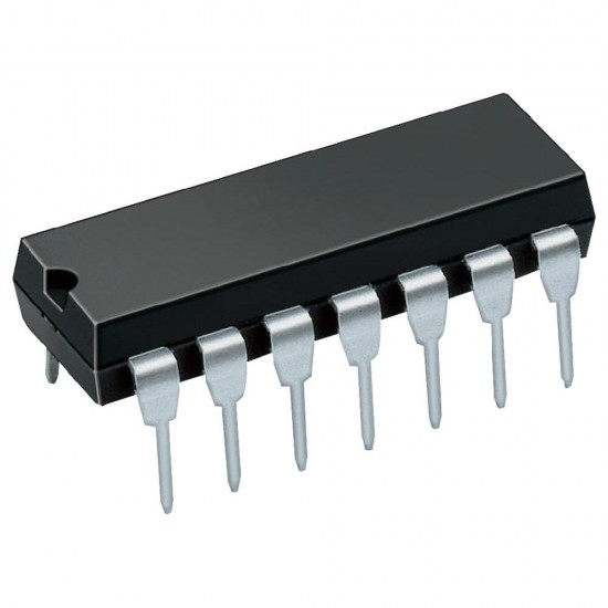
- Stock: In Stock
- Model: 74HC10
- Weight: 1.05g
- Dimensions: 19.25mm x 6.35mm x 3.35mm
- SKU: 1073
High-Speed Silicon-Gate CMOS Architecture
The 74HC10 is an advanced silicon-gate CMOS triple 3-input NAND gate logic integrated circuit designed to deliver the rapid switching speeds associated with low-power Schottky TTL (LSTTL) logic while maintaining the negligible static power consumption inherent to standard CMOS logic circuits. The internal structure comprises three independent gate cells, each operating according to the Boolean logic equation Y = NOT (A AND B AND C). Utilizing advanced semiconductor process nodes, the IC achieves propagation delay times (tPD) as fast as 9 ns at 4.5V operation, making it ideal for high-throughput digital signal processing, synchronous bus interface networks, and fast combinational logic decoding.
Electrical Characteristics, Voltage Versatility, and Output Drive
Designed to operate across a versatile power supply range from 2.0V to 6.0V, the 74HC10 provides seamless logic compatibility across legacy 5V TTL systems, standard 3.3V microcontroller buses, and 2.0V low-power battery-operated electronic devices. The device features balanced push-pull outputs capable of sourcing and sinking up to 5.2mA at 6V (4mA at 4.5V), directly supporting high fan-out topologies up to 10 LSTTL equivalent loads. Integrated input hysteresis provides enhanced noise immunity, preventing false triggering caused by ringing or slow input signal transition edges. Furthermore, ultra-low input bias currents (less than 1 uA) minimize loading on predecessor driver stages, ensuring high signal fidelity across multi-tier digital architectures.
Robust Circuit Protection and Low Power Efficiency
The integrated circuit incorporates internal ESD protection networks capable of withstanding human body model (HBM) discharges exceeding 2000V across all input and output pins. Static power consumption is strictly minimized, drawing an extremely low quiescent supply current (ICC max of 20 uA at room temperature), making it exceptionally suited for energy-constrained battery powered embedded hardware. The high noise immunity threshold—typically 30 percent of the supply voltage—ensures reliable operation in high-noise industrial environments, preventing data corruption during fast switching transients or logic gate toggling.
Application Use-Cases and DIP-14 Physical Packaging
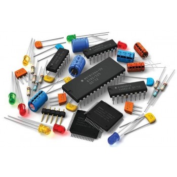
Housed in a standard 14-pin Dual In-Line Package (DIP-14) with 0.1-inch (2.54mm) pin pitch spacing, this device is engineered for rapid prototyping on solderless breadboards, universal matrix boards, and traditional through-hole printed circuit board assembly. Typical application scenarios include hardware address decoding for memory map partitioning, complex logic pattern recognition, system reset enable signal routing, bus collision mitigation, and multiphase clock signal conditioning. It serves as a foundational building block in embedded control units, telecommunications switching gear, industrial automation control loops, and educational digital design labs.