



















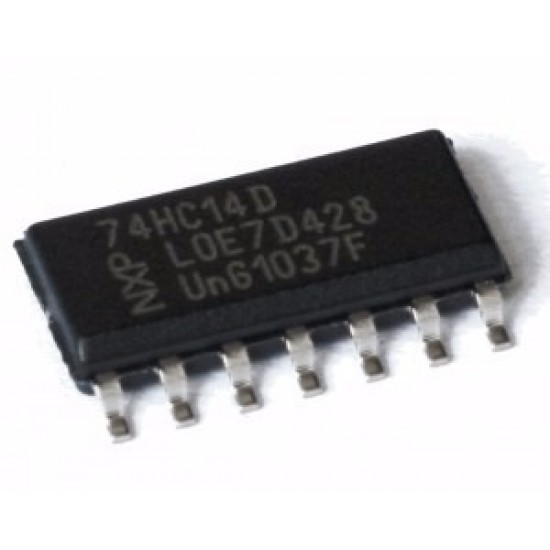
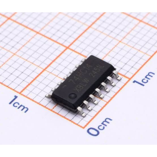


- Stock: In Stock
- Model: 74HC14 SMD
- Weight: 0.14g
- Dimensions: 8.65mm x 6.00mm x 1.65mm
- SKU: 1598
High-Speed CMOS Hex Inverting Schmitt Trigger Architecture
The 74HC14 is a premium-grade, high-speed silicon-gate CMOS logic device incorporating six independent inverting buffer channels, each equipped with dedicated Schmitt trigger inputs. Operating across a wide VCC supply voltage range of 2.0V to 6.0V, this integrated circuit is engineered to seamlessly transform slow-moving, degraded, or electrically noisy analog and digital input signals into crisp, well-defined rectangular output waveforms. By utilizing an advanced CMOS silicon-gate process, the device achieves high-speed propagation performance comparable to Low-power Schottky TTL (LSTTL) logic while maintaining the ultralow static power dissipation characteristic of standard CMOS circuitry.
Hysteresis Dynamics and Signal Conditioning Performance
At the core of each gate within the 74HC14 is an optimized Schmitt trigger differential input stage that establishes distinct positive-going and negative-going threshold voltages. This fundamental architectural feature generates a typical input hysteresis voltage differential of 0.8V to 1.4V at a 4.5V operating rail, effectively eliminating false output triggering, chatter, and spurious oscillation caused by slow input signal rise and fall times. The built-in noise margin differential guarantees extreme noise immunity, making the device ideal for conditioning signals originating from high-impedance sensors, long cable runs, mechanical contact switches, and optocouplers.
Electrical Characteristics and Driving Capability
Each channel in the 74HC14 boasts robust output driver stages capable of sinking and sourcing up to 5.2 mA at 6.0V, enabling direct interfacing with standard TTL logic families, microcontrollers, and low-power peripherals. The device exhibits extremely low input bias currents, preserving signal integrity in high-impedance timing networks. Featuring typical propagation delays of just 12 ns at VCC = 4.5V and a maximum ambient operating temperature range of -40 to +125 degrees Celsius, this component reliably executes signal restoration under severe environmental and thermal stress.
Engineering Application Use-Cases and System Integration
The versatile functional profile of the 74HC14 makes it a critical building block across diverse embedded and industrial hardware systems. Key engineering applications include multi-channel mechanical switch contact debouncing, astable and monostable relaxation oscillators, high-frequency pulse-shaping modules, line receivers in noisy EMI environments, and clock signal regeneration networks. Encapsulated in a standard SOIC-14 surface-mount footprint, the IC minimizes parasitic capacitance and PCB trace lengths, delivering high functional density for modern high-reliability printed circuit boards.