



















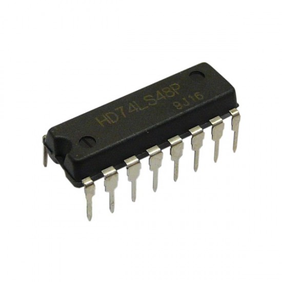
- Stock: In Stock
- Model: HD74LS48P
- Weight: 1.20g
- Dimensions: 19.69mm x 6.35mm x 4.57mm
- SKU: 738
Renesas HD74LS48P Technical Overview and Architecture
The Renesas HD74LS48P is a monolithic integrated circuit fabricated using Low-Power Schottky (LS) TTL logic technology. It functions as a BCD-to-7-Segment Decoder and Driver designed to decode 4-bit Binary Coded Decimal inputs (A, B, C, D) into active-high outputs tailored for directly driving standard 7-segment display digits or external logic interfaces. By utilizing Low-Power Schottky processing, the device achieves a optimal balance between fast propagation delay times and reduced static power dissipation compared to standard 74xx series logic circuits.
Logic Control and Multi-Digit Cascade Mechanics
The internal architecture incorporates versatile logic control pins designed to simplify complex multi-digit visual display arrays. The Ripple Blanking Input (RBI) works in tandem with the Ripple Blanking Output (RBO) to enable automatic leading and trailing zero suppression across cascading display configurations. When a display digit processes a value of zero with RBI held low, the segments are automatically blanked, and a low signal propagates to the downstream RBO pin to blank preceding zeros. Furthermore, the device features a dedicated Lamp Test (LT) pin that overrides inputs to illuminate all seven segments simultaneously for diagnostic display validation, as well as a multi-function Blanking Input (BI/RBO) pin capable of direct intensity regulation using Pulse-Width Modulation (PWM) signals.
Electrical Characteristics and Operating Thresholds
Operating within a tightly regulated VCC range of 4.75V to 5.25V with a nominal 5.0V power rail, the HD74LS48P delivers active-high outputs that contain internal pull-up resistors. These outputs are optimized for interfacing directly with common-cathode LED 7-segment displays when paired with appropriate external current-limiting series resistors. The logic inputs feature standard TTL voltage thresholds, providing robust noise margins and seamless integration with standard 5V logic controllers, microcontrollers, and discrete flip-flop registers across an operational commercial temperature range of 0 degrees Celsius to +70 degrees Celsius.
Circuit Integration and System Applications
Encapsulated in a industry-standard 16-pin Dual In-line Package (DIP-16) with standard 0.1-inch pin pitch spacing, the HD74LS48P is ideal for through-hole PCB designs, solderless breadboards, and prototyping boards. Common application scenarios include digital panel meters, frequency counters, industrial automation instrumentation, event timers, electronic clocks, educational logic circuit trainers, and vintage digital hardware restoration projects where low component counts and reliable hardware decoding are essential.