Menu
Your Cart
NOTICE: We have Fully discontinued physical walk-in customer service, RFQ, and LPO processing. Nerokas is now a FULLY DIGITAL ONLINE STORE, and our virtual assistant, Ginō AI, is here to help you navigate and checkout. Just ADD your Items to cart and type CHECKOUT on Ginō. Please note that corporate customers must register a corporate account to ensure proper Digital eTIMS/VAT processing.

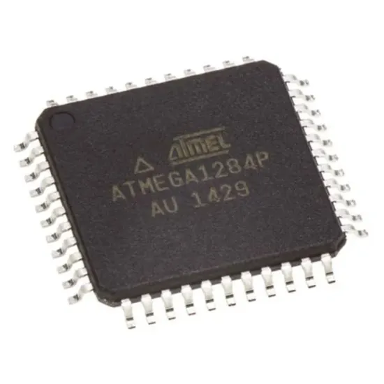
ATMEGA1284P-AU - 8-bit AVR

ATMEGA1284P-AU - 8-bit AVR
KES 1,800.00
  • Stock: In Stock
  • Model: ATMEGA1284P-AU
  • SKU: 3807

Product Overview and Architecture

The Microchip ATmega1284P-AU is a flagship high-performance, low-power 8-bit AVR RISC-based microcontroller engineered to handle memory-intensive and computationally demanding embedded applications. Built upon an advanced Harvard architecture, the ATmega1284P executes instructions in single clock cycles, yielding processing throughputs approaching 1 MIPS per megahertz. This exceptional processing density enables hardware designers to optimize system performance against overall power draw, operating from supply voltages ranging from 1.8V to 5.5V at speeds up to 20 MHz.

What sets the ATmega1284P apart within the MegaAVR family is its vast memory allocation combined with low power features. It houses 128 KB of in-system programmable flash memory, 4 KB of EEPROM, and an impressive 16 KB of internal SRAM. The unusually large 16 KB SRAM buffer eliminates memory bottlenecks frequently encountered in 8-bit systems, enabling developers to run real-time operating systems (RTOS), maintain substantial communications buffers, drive graphic displays, and compute complex signal processing algorithms without resorting to external memory expansion.

Core CPU and Silicon Features

The CPU core combines a rich instruction set of 131 powerful instructions with 32 general-purpose 8-bit working registers. All 32 registers are connected directly to the Arithmetic Logic Unit (ALU), allowing two independent registers to be accessed in a single instruction executed in one clock cycle. This architectural topology delivers up to ten times faster throughput than conventional CISC microcontrollers.

Equipped with Microchip proprietary picoPower technology, the ATmega1284P features dynamic power reduction mechanisms. It supports six software-selectable power-saving modes: Idle, ADC Noise Reduction, Power-save, Power-down, Standby, and Extended Standby. Integrated features such as brown-out detection (BOD), an ultra-low-power watchdog timer, a real-time counter (RTC), and software-configurable Power Reduction Registers (PRR) allow total power draw to be minimized down to microamp levels during sleep, making it ideal for battery-operated field equipment.

Integrated Peripheral Suite

The ATmega1284P-AU package in TQFP-44 provides 32 software-programmable input/output (I/O) lines arranged across four 8-bit ports (Port A through Port D). The peripheral set includes two fully independent hardware USARTs supporting full-duplex asynchronous serial communication, hardware flow control, and Master SPI modes. It incorporates an SPI serial interface for high-speed synchronous communications and a 2-wire Serial Interface (TWI) compatible with I2C and SMBus protocols.

Analog signal acquisition is handled by an 8-channel, 10-bit Analog-to-Digital Converter (ADC). The ADC includes an analog multiplexer supporting differential voltage inputs with programmable gain stages of 1x, 10x, and 200x, facilitating direct interfacing with low-amplitude sensors without external instrumentation amplifiers. On-chip timing services consist of two 8-bit Timer/Counters and two 16-bit Timer/Counters, each equipped with separate prescalers, compare modes, and hardware Pulse Width Modulation (PWM) channels.

TQFP-44 Pinout Layout and Signal Description

The 44-pin Thin Quad Flat Pack (TQFP) surface-mount package balances high pin-density with ease of PCB layout. Key pin groups include:

Power and Ground: VCC (Pins 5, 17, 38) provides digital core power; GND (Pins 6, 18, 28, 39) serves as system ground. AVCC (Pin 27) supplies power to Port A and the ADC, requiring external decoupling to VCC through an LC filter for precision analog measurements. AREF (Pin 29) provides the analog reference voltage input.

Port A (PA0 to PA7 / Pins 37 to 30): Serves as an 8-bit bi-directional I/O port with internal pull-up resistors and acts as the analog inputs (ADC0 to ADC7) for the A/D converter.

Port B (PB0 to PB7 / Pins 40 to 44, Pins 1 to 3): Bi-directional I/O pins providing alternative functions including Timer/Counter outputs, external interrupts, and the Serial Peripheral Interface (SPI) pins: PB5 (MOSI), PB6 (MISO), PB7 (SCK), and PB4 (SS).

Port C (PC0 to PC7 / Pins 19 to 26): Functions as a bi-directional I/O port. Pins PC0 (SCL) and PC1 (SDA) host the 2-Wire Interface (I2C), while PC2 to PC5 double as the IEEE 1149.1 compliant JTAG test interface (TCK, TMS, TDO, TDI) used for boundary-scan and on-chip debugging.

Port D (PD0 to PD7 / Pins 8 to 15): Provides bi-directional I/O lines and houses the dual USART interfaces: PD0 (RXD0), PD1 (TXD0), PD2 (RXD1/INT0), PD3 (TXD1/INT1), alongside high-speed PWM outputs and external interrupt pins.

Application Use-Cases and Hardware Configuration

1. Industrial Modbus and RS-485 Communication Gateway

In industrial automation systems, the dual hardware USARTs enable the ATmega1284P to act as a dual-channel protocol translator or RS-485 gateway. USART0 (PD0/RXD0, PD1/TXD0) connects to a isolated RS-485 transceiver for master controller polling, while USART1 (PD2/RXD1, PD3/TXD1) connects to a local sensor array. Pin PD4 is configured as a general-purpose output driving the Driver Enable (DE) and Receiver Enable (RE) lines of the RS-485 transceiver. The 16 KB SRAM allows extensive modbus frame buffering, prevent data overrun errors during high-baud-rate bursts.

2. Multi-Channel Environmental Data Logger

The ATmega1284P is well suited for remote weather stations and industrial data monitoring. The 8-channel ADC (PA0 to PA7) interfaces with analog sensors such as thermistors, light sensors, and gas detectors. An external SPI flash memory chip connects to PB5 (MOSI), PB6 (MISO), and PB7 (SCK) to store data logs, while PC0 (SCL) and PC1 (SDA) connect to a Real-Time Clock (RTC) chip over I2C for accurate timestamping. The large 128 KB Flash memory houses deep logging libraries and data formatting software.

3. Advanced Battery Management System (BMS)

For high-capacity lithium battery packs, the microcontrollers differential ADC mode provides precise monitoring. Pins PA0 and PA1 are configured as differential inputs with 10x or 200x gain to measure battery current across a low-side shunt resistor. Pins PA2 through PA7 measure cell voltages via resistive divider networks. The microcontrollers I2C bus (PC0/SCL, PC1/SDA) communicates battery metrics to a host system via SMBus, while hardware PWM pins (PD4, PD5) control active cell-balancing switches.

4. Quad-Axis CNC Motion and Stepper Motor Control

CNC machinery requires simultaneous multi-axis pulse generation. The two 16-bit timers (Timer1 and Timer3) and two 8-bit timers generate highly predictable step and direction pulses. Pins PD4 (OC1B), PD5 (OC1A), PB3 (OC0A), and PB4 (OC0B) supply high-frequency PWM or step pulses to stepper drivers. Port C pins (PC2 to PC5) process quadrature encoder signals via pin-change interrupts (PCINT18-PCINT21) to maintain real-time positional tracking.

5. Embedded Digital Audio Synthesizer

Leveraging its 16 KB SRAM, the ATmega1284P can perform real-time wave-table audio synthesis and digital signal generation. Audio sample tables are loaded from internal Flash or an SD Card attached via SPI (PB5-PB7). Timer1 and Timer2 are configured for high-speed phase-correct PWM output on PD4 and PD5, driving an external low-pass filter to generate dynamic analog audio waveforms without requiring an external DAC.

6. Smart Energy Metering System

Smart meters monitor current, line voltage, active power, and power factor in real time. The differential ADC pins (PA0/PA1) amplify signal levels directly from current transformers (CTs). Interrupt pins PD2 (INT0) and PD3 (INT1) track zero-crossing events on the AC line to derive power factor values. Real-time calculations are saved to onboard 4 KB EEPROM to prevent data loss during power outages, and recorded data is transmitted via UART (PD1/TXD0) to an optical or wireless modem.

7. Long-Range LoRa/Zigbee Telemetry Node

For agricultural or smart city sensing, the ATmega1284P pairs with a RF module. Hardware SPI (PB4 to PB7) controls a LoRa or Zigbee transceiver. External interrupt pin PD2 (INT0) wakes the MCU from deep Power-down mode upon packet reception. Sensor data collected across Port A (PA0-PA7) is packetized and transmitted. Operating at 3.3V, the picoPower system consumes less than 1 microamp in sleep mode, enabling multi-year battery operational lifespans.

8. Embedded JTAG Debugger and ISP Programmer

The integrated JTAG interface (PC2/TCK, PC3/TMS, PC4/TDO, PC5/TDI) allows the ATmega1284P to operate as a dedicated hardware programmer and target debugger. Connected to a PC host through USART0 (PD0/PD1), the board can execute standard AVR instruction sets, flash programming routines, and boundary scan testing to program downstream target microcontrollers using SPI pins (PB5/MOSI, PB6/MISO, PB7/SCK, PB4/SS).

Ginō Ginō AI - Nerokas AI Assistant
✕
Jambo! I am Ginō, a Nerokas AI Assistant and Africa's best Open Hardware Facilitator AI agent here to help. In order to serve you better and to help me give you accurate shipping estimates as we begin, could you please tell me your name and your location/city?

You can also ask about any hardware or type I'd like to order, I am looking for..., you can also LIST all SKUs & Quantity of desired items from our website here for me to help you Checkout automatically at anytime to fast-track your requests and orders.