Menu
Your Cart
NOTICE: We have Fully discontinued physical walk-in customer service, RFQ, and LPO processing. Nerokas is now a FULLY DIGITAL ONLINE STORE, and our virtual assistant, Ginō AI, is here to help you navigate and checkout. Just ADD your Items to cart and type CHECKOUT on Ginō. Please note that corporate customers must register a corporate account to ensure proper Digital eTIMS/VAT processing.

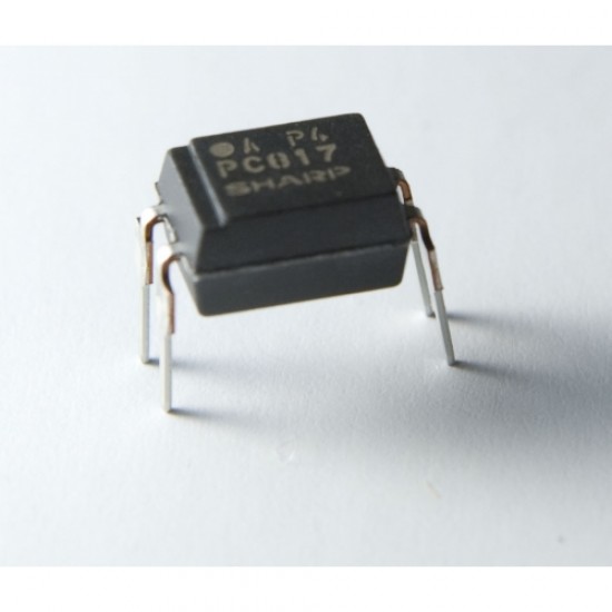
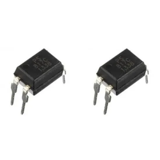
PC817 – Optoisolator / Optocoupler, DIP4

PC817 – Optoisolator / Optocoupler, DIP4
Top Seller
PC817 – Optoisolator / Optocoupler, DIP4
KES 30.00
  • Stock: In Stock
  • Model: PC817
  • Weight: 0.30g
  • Dimensions: 4.60mm x 6.50mm x 4.50mm
  • SKU: 1009
This product has a minimum quantity of 5

Product Overview and Architecture

This high-performance single-channel phototransistor optocoupler delivers robust galvanic isolation in a compact 4-pin Dual In-line Package (DIP-4). Designed to bridge disparate voltage domains while completely isolating sensitive digital electronics from hazardous high-voltage transients, this component incorporates an Infrared Light-Emitting Diode (GaAs IR LED) optically coupled to a high-sensitivity NPN silicon phototransistor. By transmitting signals entirely through optical radiation, physical electrical contact between the primary input circuit and the secondary output circuit is eliminated, preventing ground loops, common-mode noise propagation, and high-voltage spikes from compromising control logic.

Featuring an exceptional dielectric isolation rating of 5000V RMS (5kV), a collector-emitter breakdown voltage (Vceo) of 80V, and a high Current Transfer Ratio (CTR) ranging between 200% and 400%, this device is an ideal choice for power supply regulation, industrial control logic, and micro-controller interface isolation. The DIP-4 package allows for both standard through-hole PCB assembly and socket insertion, making it highly versatile for rapid prototyping and high-reliability production environments.

Comprehensive Technical Specifications

The device operates with a nominal forward input current of 20mA, while supporting a maximum continuous forward current (If) of 50mA. On the output side, the phototransistor handles a maximum collector current (Ic) of 20mA and maximum power dissipation of 200mW across its operational temperature range of -30 degrees Celsius to +100 degrees Celsius. The switching dynamics are characterized by balanced 18-microsecond rise times and 18-microsecond fall times, making it exceptionally suited for low-to-medium frequency pulse transmission, switching control, and general-purpose logic level translation.

The physical geometry conforms to international DIP standards with an outside width of 6.5mm, external depth of 4.58mm, external body height of 3.5mm, lead pitch of 2.54mm, and row-to-row pitch of 7.62mm. The device complies fully with UL recognition safety standards and contains no SVHC (Substances of Very High Concern), matching stringent global environmental regulations.

Pinout Architecture and Terminal Configuration

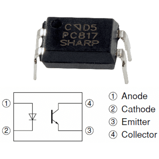
The 4-pin DIP footprint is optimized for maximum spatial efficiency and functional separation between high-voltage and low-voltage PCB layout zones:

Pin 1: Anode (Input Side)
The positive terminal of the internal Gallium Arsenide (GaAs) infrared LED. Driving current into this pin relative to Pin 2 forward-biases the internal LED, causing it to emit infrared light proportional to the forward current. An external series current-limiting resistor must be connected to Pin 1 to maintain input current within safe operating limits (typically 5mA to 20mA).

Pin 2: Cathode (Input Side)
The negative ground return terminal for the internal IR LED. Connecting this pin to the primary control circuit ground completes the input current path. The isolation barrier physically separates Pin 1 and Pin 2 from Pins 3 and 4 by a high-dielectric epoxy resin layer, maintaining 5kV continuous isolation safety.

Pin 3: Emitter (Output Side)
The emitter terminal of the internal NPN silicon phototransistor. In standard open-collector logic circuits, Pin 3 is connected to the secondary side system ground. When photon energy strikes the base region of the phototransistor, collector-to-emitter conduction occurs, allowing current to flow to Pin 3.

Pin 4: Collector (Output Side)
The collector terminal of the internal NPN phototransistor. Typically connected to a secondary DC supply rail (up to 80V) via a pull-up resistor. When the internal LED illuminates, the collector voltage drops toward the emitter potential, asserting a active-low digital signal or modulating an analog feedback voltage.

Principles of Operation

The optocoupler operates on the principle of photo-conduction across a optical channel. When a control signal drives current through the input LED (Pins 1 and 2), electron-hole recombination within the GaAs semiconductor junction emits photons with a peak wavelength tuned precisely to the absorption spectrum of the output phototransistor's base region. These photons traverse the internal insulating barrier and penetrate the silicon base of the phototransistor, generating electron-hole pairs via the photoelectric effect.

The generated photo-current acts as base drive current, causing the phototransistor to transition from a non-conducting cutoff state into a conducting active or saturated state. Because the Current Transfer Ratio (CTR) is rated at 200% to 400%, an input current of 5mA can yield output collector currents between 10mA and 20mA. This amplification capability permits direct interfacing with digital logic gates, microcontroller GPIOs, and peripheral switching transistors without requiring intermediate amplification stages.

Application Use-Cases

1. Switch-Mode Power Supply (SMPS) Isolated Feedback Loops
In offline switch-mode converters, high-voltage primary circuits must be isolated from user-accessible secondary output rails. The optocoupler is placed across the isolation boundary, working in tandem with a precision shunt regulator (such as a TL431). The secondary voltage drives the optocoupler's internal LED, which dynamically adjusts the phototransistor's collector current on the primary side. This controls the Pulse-Width Modulation (PWM) controller's feedback pin, stabilizing the output voltage while maintaining full 5kV safety isolation between AC mains and secondary DC loads.

2. Microcontroller Digital Input Isolation in Industrial Environments
Industrial control panels frequently operate with 24V DC logic levels, subject to severe electromagnetic interference, motor back-EMF, and inductive switching spikes. Connecting these signals directly to a 3.3V or 5V microcontroller risks immediate silicon damage. By routing the 24V line through a current-limiting resistor into Pin 1 of the optocoupler, the MCU pin connects safely to Pin 4 with a 10k pull-up resistor. High-voltage spikes on the factory floor are blocked by the 5kV dielectric barrier, safeguarding sensitive control electronics.

3. Solid-State Relay (SSR) Gate/Base Triggering
In high-power AC and DC switching equipment, this optocoupler acts as an optically isolated driver for power MOSFETs or Triacs. The low-power micro-controller output triggers the optocoupler LED, while the phototransistor collector switches a high-voltage gate drive circuit. This configuration prevents high power rail transients or phase-angle switching spikes from propagating back into the sensitive low-voltage control board.

4. Industrial Programmable Logic Controller (PLC) I/O Modules
Programmable Logic Controllers require multi-channel isolation to prevent ground loops between interconnected industrial sensors and field actuators. Utilizing this DIP-4 optocoupler on every discrete I/O channel creates independent isolation zones. Ground potential differences between disparate machinery components are absorbed across the isolation gap, preventing parasitic currents from corrupting system data transmission.

5. Zero-Crossing Detector Circuits for Mains Phase Control
For dimming control, heater power regulation, and AC motor speed modification, microcontrollers must detect when the utility AC voltage passes through zero volts. A bridge rectifier converts the AC waveform to full-wave pulsating DC, which drives the optocoupler input. The phototransistor pulses low every time the mains voltage drops below the LED forward voltage threshold, providing an optically isolated zero-cross sync pulse directly to an interrupt pin on the microprocessor.

6. High-Voltage Battery Management Systems (BMS)
Electric vehicle battery packs and stationary energy storage banks connect hundreds of cells in series, creating common-mode voltages reaching several hundred volts. Monitoring individual cell module telemetry requires isolated communications. This optocoupler acts as an isolated level shifter, translating status signals from high-potential battery cell monitors down to the central earth-grounded BMS controller without creating hazardous high-voltage short circuits.

7. Audio Equipment Ground-Loop Elimination
System ground loops in professional audio networks introduce noticeable 50Hz/60Hz mains hum and digital clock noise into sensitive analog signal paths. Placing an optocoupler in digital audio transmission lines (such as MIDI or proprietary control protocols) breaks the physical ground continuity between audio equipment chassis. This preserves signal integrity and eliminates hum while maintaining data throughput.

8. Isolated ADC and Sensor Instrumentation Interfaces
In precision medical monitor designs, industrial process transducers, and high-side current sensing circuits, sensor front-ends must operate floating at elevated voltages. This phototransistor optocoupler transmits digitized sensor frequency output or optical pulse-train signals across the isolation barrier to processing units without altering baseline calibration or introducing high-voltage hazards to operators.

PCB Layout, Creepage, and Design Optimization

To maximize the 5kV isolation safety of this component, careful attention must be given to printed circuit board routing. Standard design practices mandate placing a physical isolation slot (air gap cut) directly beneath the optocoupler body between Pins 1-2 and Pins 3-4. This maximizes PCB surface creepage distance and air clearance, preventing surface tracking or high-voltage arc-over under humid or contaminated conditions.

Additionally, designers should optimize the output pull-up resistor value relative to the desired switching frequency. Selecting a smaller resistor value decreases phototransistor saturation storage time, effectively reducing the 18-microsecond rise and fall times to achieve higher signal speeds. Ensure that peak current demands on Pin 1 remain within the safe operating envelope, accounting for long-term LED efficiency degradation over extended thermal operating cycles.

Official Resources & Manuals

Ginō Ginō AI - Nerokas AI Assistant
✕
Jambo! I am Ginō, a Nerokas AI Assistant and Africa's best Open Hardware Facilitator AI agent here to help. In order to serve you better and to help me give you accurate shipping estimates as we begin, could you please tell me your name and your location/city?

You can also ask about any hardware or type I'd like to order, I am looking for..., you can also LIST all SKUs & Quantity of desired items from our website here for me to help you Checkout automatically at anytime to fast-track your requests and orders.