



















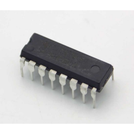
- Stock: In Stock
- Model: 74HC157
- Weight: 1.20g
- Dimensions: 19.25mm x 8.25mm x 4.57mm
- SKU: 1080
High-Speed Logic Data Selector Architecture
The 74HC157 is a high-speed Silicon-gate CMOS quad 2-input multiplexer engineered for high-performance digital signal routing, bus switching, and parallel data selection. Operating as a 4-bit dual-source selector, this integrated circuit dynamically routes 4 bits of parallel data from one of two selectable input banks (1A to 4A or 1B to 4B) directly to corresponding non-inverting outputs (1Y to 4Y). Master control is managed via a single Data Select input pin (S) that determines which input bank is gated through to the output stage. An Active-LOW Enable or Strobe input pin (E) acts as an overriding master control; when driven HIGH, the Enable line forces all four Y outputs LOW regardless of active states on the data inputs, simplifying multi-device bus arbitration and hardware power-down sequences.
LSTTL Compatibility and Low-Power CMOS Performance
Fabricated with advanced Si-gate CMOS processing, the 74HC157 achieves propagation delays of approximately 11ns at 5V, matching the performance metrics of classic Low-power Schottky TTL (LSTTL) logic while maintaining ultra-low static power consumption (maximum quiescent current of 4uA). Pin-compatible and logic-level compatible with 74 series LSTTL devices, it integrates directly into retrofitted processing boards or modernized digital logic systems. The component operates reliably across a wide VCC supply voltage spectrum from 2.0V to 6.0V. Its robust output stages provide high drive capability (up to +/- 5.2mA sink/source current at 4.5V and +/- 7.8mA at 6.0V), offering excellent noise immunity and high fan-out capability to drive capacitive loads or backplane logic networks.
Deep Technical Application Use-Cases
This quad 2:1 multiplexer excels in complex embedded hardware architectures where parallel data paths must be multiplexed without introducing CPU cycle latency. Key implementations include memory bank address switching, parallel printer port arbitration, hardware lookup table logic generation, and multi-channel sensor signal multiplexing. In microcontroller and FPGA setups, the 74HC157 is commonly used to multiplex address lines between primary and backup RAM banks, switch data buses between high-speed peripherals, or route dual clock signals to synchronized state machines while preserving clock edge integrity.
DIP-16 Package Specifications and Thermal Resilience
Housed in a standard 16-pin Dual In-line Package (300 mil width with a 2.54mm lead pitch), the IC allows easy integration into through-hole printed circuit boards, IC sockets, and solderless prototyping breadboards. Engineered for demanding thermal operational profiles, the 74HC157 features an extended industrial operating temperature range spanning from -55 degrees Celsius to 125 degrees Celsius. Internal ESD protection diodes on all inputs safeguard the device against electrostatic discharges up to 2000V Human Body Model (HBM), making it a high-reliability component for automotive modules, industrial automation controllers, and laboratory test instruments.