Menu
Your Cart

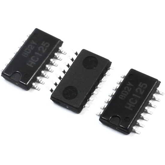
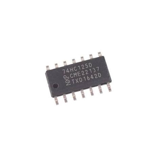
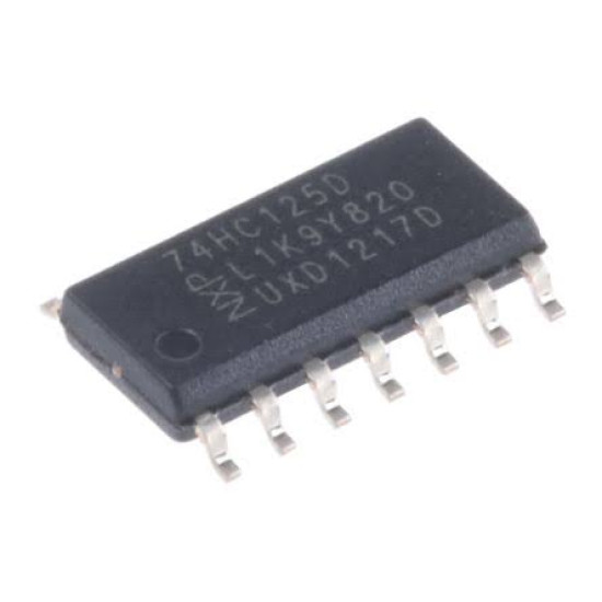
74HC125D - IC, BUFFER, CMOS, SMD

74HC125D - IC, BUFFER, CMOS, SMD
KES 100.00
  • Stock: In Stock
  • Model: 74HC125D
  • Weight: 1.04g
  • Dimensions: 8.65mm x 6.00mm x 1.65mm
  • SKU: 1150

Overview and Silicon Architecture

The 74HC125 is a high-speed CMOS quadruple buffer and line driver engineered for flexible operation across a wide supply voltage range of 2.0V to 6.0V. Fabricated using advanced silicon-gate CMOS technology, this integrated circuit combines the high noise immunity and low power dissipation characteristic of CMOS devices with driving performance matching Low-Power Schottky TTL logic family outputs. The IC incorporates four independent, non-inverting buffer stages, each controlled by a dedicated active-low Output Enable control pin. When an Output Enable pin is asserted low, the corresponding signal buffer passes input logic levels directly to the output. Conversely, driving the control pin high places the output into a high-impedance state, effectively isolating the driver stage from the system interconnect.

Electrical Characteristics and Dynamic Performance

Engineered for high-frequency signal switching and robust drive performance, the 74HC125 delivers rapid propagation delays typically around 11 ns at a 5V VCC supply with a 50 pF load. Each output buffer is capable of driving up to 15 LSTTL loads, providing a symmetric source and sink output current capacity of plus or minus 6 mA at 4.5V. The high-impedance 3-state outputs exhibit negligible leakage current of less than 5 microamps, minimizing total bus loading and preventing unwanted thermal dissipation in dense multi-transceiver architectures. The logic inputs feature standard CMOS thresholds and integrated electrostatic discharge protection networks exceeding 2000V Human Body Model, ensuring resilience against transient voltage spikes and latch-up events in industrial environments.

System Integration and Application Use-Cases

The active-low control scheme of the 74HC125 makes it a fundamental building block for modern microcontrollers, digital signal processors, and FPGA systems. It is extensively utilized in shared data and address bus architectures, memory expansion interfaces, and SPI bus line isolation modules. By multiplexing multiple output drivers onto a single shared transmission line, engineers can prevent bus contention while maintaining clean signal integrity over extended printed circuit board traces. Beyond traditional bus multiplexing, the device serves exceptionally well as a signal repeater, capacitive load line driver, and input voltage level isolator across mixed-voltage system domains operating within the 2V to 6V window.

Package and Thermal Reliability

Housed in an industry-standard 14-pin Small Outline Integrated Circuit (SOIC-14) surface-mount package, the 74HC125 optimizes board real estate while maintaining reliable thermal performance. The component is fully specified for operation across an extended industrial operating temperature range from -40 degrees C to +125 degrees C. Featuring a Moisture Sensitivity Level rating of MSL 1, the device provides unlimited floor life under standard manufacturing conditions, ensuring complete compatibility with automated surface-mount technology pick-and-place assembly and lead-free reflow soldering profiles.

Ginō Ginō AI - Nerokas AI Assistant
Jambo! I am Ginō, a Nerokas AI Assistant and Africa's best Open Hardware Facilitator AI agent here to help. In order to serve you better and to help me give you accurate shipping estimates as we begin, could you please tell me your name and your location/city?

You can also ask about any hardware or type I'd like to order, I am looking for..., you can also LIST all SKUs & Quantity of desired items from our website here for me to help you Checkout automatically at anytime to fast-track your requests and orders.