


















- Stock: In Stock
- Model: 74HC14
- Weight: 1.02g
- Dimensions: 19.25mm x 7.92mm x 4.57mm
- SKU: 1300
Overview and Architecture
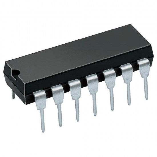
The 74HC14 is a high-speed silicon-gate CMOS integrated circuit featuring six independent inverting logic gates, each equipped with integrated Schmitt-trigger inputs. It combines the exceptionally low power dissipation and high noise immunity characteristic of standard CMOS logic with the drive capability of up to 10 Low-Power Schottky TTL (LS-TTL) loads. Fully pinout and functionally compatible with the standard 74LS logic family, the 74HC14 serves as a seamless upgrade path for legacy designs requiring improved noise performance, expanded operating voltage limits, and significantly reduced standby power consumption. Fabricated using advanced silicon-gate CMOS technology, the device achieves exceptional operational stability and long-term reliability across broad industrial temperature ranges.
Advanced Schmitt-Trigger Action and Hysteresis
Unlike standard CMOS logic gates that suffer from output oscillation and excessive supply current draw when exposed to slowly transitioning input edges, the 74HC14 features engineered internal input hysteresis. It offers a typical hysteresis voltage of 0.9V at a supply voltage of 4.5V and up to 1.4V at 6.0V. This threshold differential allows the device to transform slow-changing, noisy, or distorted analog input signals into clean, sharp, jitter-free digital square waves. The positive-going threshold and negative-going threshold ensure distinct, non-overlapping switching points, completely eliminating ambiguous logic regions and preventing false triggering caused by electromagnetic interference or supply ripple voltage.
Electrical Characteristics and ESD Protection
Designed for operating versatility across diverse power domains, the 74HC14 functions reliably across a wide supply voltage range from 2.0V to 6.0V. It achieves a fast typical propagation delay of just 13 ns at 4.5V, making it well suited for high-frequency signal conditioning and timing applications. System power efficiency is maximized with a maximum quiescent supply current of only 20 uA for the IC and an ultra-low input leakage current of 1 uA maximum. To ensure structural integrity in challenging electrical environments, all inputs are reinforced with robust electrostatic discharge protection comprising internal clamping diodes connected to VCC and Ground, capable of withstanding ESD events exceeding 2000V Human Body Model performance.
Applications and Hardware Implementation Context
The unique hysteresis characteristics of the 74HC14 make it an essential building block for signal conditioning circuits across embedded systems. Key implementation use-cases include mechanical switch debouncing for pushbuttons and rotary encoders, wave-shaping for slow edge-rate optocouplers and sensors, astable RC pulse generators, simple relaxation oscillators, and noise-immune line receivers. By serving as a robust buffer between analog sensors and high-speed digital processing units such as microcontrollers, DSPs, or FPGAs, the 74HC14 safeguards downstream logic from state instability and waveform degradation.