




















- Stock: Out Of Stock
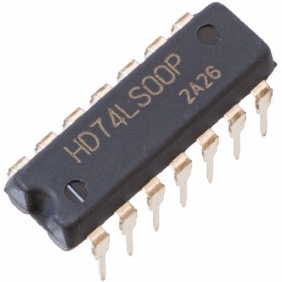
- Model: 74LS00
- Weight: 1.00g
- Dimensions: 19.30mm x 7.62mm x 4.57mm
- SKU: 256
High-Performance Low-Power Schottky Logic Architecture
The 74LS00 integrated circuit is a staple logic chip featuring four independent 2-input NAND gates built using Low-Power Schottky TTL (Transistor-Transistor Logic) technology. As a universal logic gate, a NAND gate can be configured to recreate any fundamental logic operation including AND, OR, NOT, NOR, and XOR functions. The internal Schottky diode clamping significantly enhances switching speed compared to standard TTL chips while keeping overall power consumption low, making the 74LS00 ideal for rapid digital logic execution in embedded system glue logic, educational kits, and timing control networks.
Complete Pinout and Logic Output Topology
Housed in a standard 14-pin Dual-In-Line Package (DIP-14), the 74LS00 provides a symmetrical layout designed for clean breadboard integration and printed circuit board (PCB) traces. Power is applied across Pin 14 (VCC, 5V standard) and Pin 7 (GND). Logic evaluation follows standard Active-Low NAND truth tables across four discrete internal gates: Gate 1 uses Pin 1 and Pin 2 as inputs driving Output Pin 3; Gate 2 uses Pin 4 and Pin 5 driving Output Pin 6; Gate 3 uses Pin 9 and Pin 10 driving Output Pin 8; and Gate 4 uses Pin 12 and Pin 13 driving Output Pin 11.
Electrical Characteristics and Operating Parameters
Engineered to operate reliably across standard commercial temperatures ranging from 0°C to +70°C, the 74LS00 features strict logic voltage levels. The supply voltage is rated for optimal performance at 5.0V with operational bounds between 4.75V and 5.25V. High-level input voltage (VIH) requires a minimum of 2.0V, while low-level input voltage (VIL) accepts a maximum threshold of 0.8V. The IC can sink up to 8 mA of output current (IOL) for driving downstream TTL inputs or low-power indicators, with typical propagation delays around 9 to 15 nanoseconds per gate.
Applications and Integration Scenarios
Thanks to its DIP-14 form factor, the 74LS00 can be directly inserted into standard IC sockets, breadboards, or soldered into target PCBs. Common application use cases include building cross-coupled SR flip-flops for pulse generation and switch debouncing, implementing address decoding for 8-bit microcontrollers, forming clock oscillator circuits, and creating custom combinational logic functions in digital hardware design and retrofit electronics repair.