Menu
Your Cart

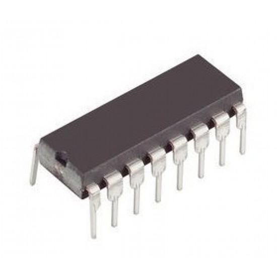
74LS195 Universal 4-Bit Shift Register IC

74LS195 Universal 4-Bit Shift Register IC
KES 150.00
  • Stock: In Stock
  • Model: 74LS195
  • Weight: 1.20g
  • Dimensions: 19.30mm x 7.62mm x 4.57mm
  • SKU: 3662

Product Overview

The 74LS195 is a high-speed 4-bit universal shift register integrated circuit engineered using low-power Schottky diode-clamped TTL process technology. Capable of typical shift frequencies up to 39 MHz with low propagation delay, this IC provides fast data manipulation and robust interfacing across standard TTL logic levels and digital microcontroller I/O lines. Its reliable architecture makes it an essential building block for digital memory systems, hardware arithmetic units, counting circuits, and high-performance communication pipelines.

Architecture and Functional Operations

This 4-bit shift register supports fully synchronous serial or parallel data transfers. Parallel data loading is executed when the active-low Parallel Enable line is driven low synchronously with a positive-going clock transition, transferring parallel inputs P0 through P3 directly to outputs Q0 through Q3. When Parallel Enable is held high, serial data entry is enabled and controlled via the first-stage J and active-low K inputs, allowing flexible shift-right operations, toggle functions, or serial data streaming. An asynchronous Master Reset line overrides all clocking and control inputs, immediately clearing all internal flip-flops and forcing outputs Q0 through Q3 to a logical low state upon activation.

Pinout and Signal Identification

Housed in a standard 16-pin dual in-line package (DIP-16), the pin layout is structured for optimal PCB signal routing: Pin 1 serves as the active-low Master Reset input; Pin 2 provides the J serial input; Pin 3 functions as the active-low K serial input; Pins 4, 5, 6, and 7 correspond to parallel data inputs P0, P1, P2, and P3; Pin 8 connects to system Ground; Pin 9 functions as the active-low Parallel Enable line; Pin 10 receives the active rising-edge Clock signal; Pin 11 yields the inverted complementary output Q3 bar for the final stage; Pins 12, 13, 14, and 15 present parallel outputs Q3, Q2, Q1, and Q0 respectively; Pin 16 connects to the main 5V VCC supply rail.

Technical Applications and Implementation

Due to its versatile logic capabilities and synchronous edge-triggered control, the 74LS195 is extensively deployed in serial-to-parallel and parallel-to-serial conversion modules, pseudorandom pattern generators, shift-left and shift-right register networks, Johnson counters, ring counters, hardware data delay lines, and memory address bus buffer circuits.

Official Resources & Manuals

Ginō Ginō AI - Nerokas AI Assistant
Jambo! I am Ginō, a Nerokas AI Assistant and Africa's best Open Hardware Facilitator AI agent here to help. In order to serve you better and to help me give you accurate shipping estimates as we begin, could you please tell me your name and your location/city?

You can also ask about any hardware or type I'd like to order, I am looking for..., you can also LIST all SKUs & Quantity of desired items from our website here for me to help you Checkout automatically at anytime to fast-track your requests and orders.