



















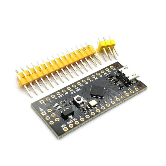
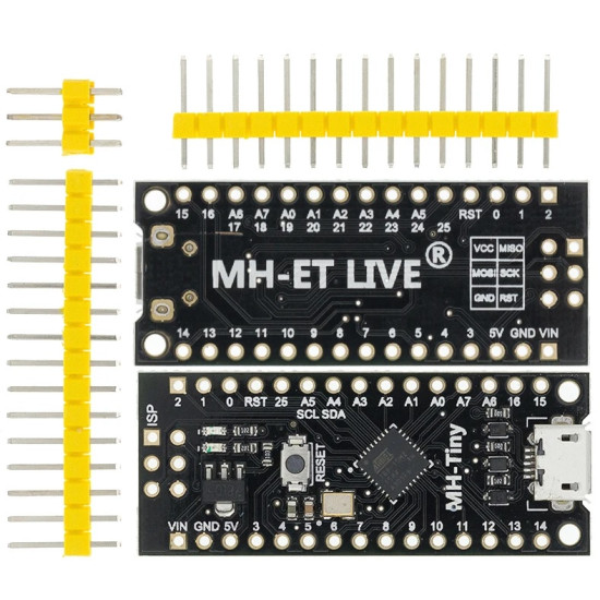


- Stock: In Stock
- Model: MH-Tiny ATTINY88 micro development board
- SKU: 3754
Comprehensive Architectural Overview
The ATTiny88 Microcontroller Development Board is an exceptionally compact, highly efficient 8-bit AVR development platform designed for embedded systems engineers, hobbyists, and OEM developers seeking a cost-effective alternative to standard Arduino Nano boards. Driven by the Microchip ATtiny88 microchip operating at an internal clock frequency of 16.0 MHz, this board packs massive digital input and output capabilities into a diminutive form factor measuring just 44.5mm by 18.3mm. Utilizing high-density surface-mount technology, this board delivers robust performance, reduced power consumption, and direct Arduino IDE toolchain compatibility, making it an outstanding choice for ultra-compact IoT projects, sensor hubs, and custom USB human interface devices.
Unlike conventional microcontroller development boards that rely on dedicated USB-to-UART bridge ICs (such as the CH340 or FT232), the ATTiny88 platform utilizes a virtual USB firmware stack (V-USB) combined with the Micronucleus bootloader. This architecture allows direct USB flashing and native low-speed USB communication without requiring dedicated peripheral interface chips, saving physical board space and significantly reducing BOM cost. The board provides 26 general-purpose input/output (GPIO) pins, an integrated 500mA voltage regulator, low-noise analog-to-digital converter lines, and standard serial bus topologies including I2C and SPI.
Microcontroller Core and Memory Topology
At the heart of the board resides the Atmel/Microchip ATtiny88 AVR 8-bit RISC-based microcontroller. Executing powerful instructions in a single clock cycle, the board achieves throughputs approaching 1 MIPS per MHz, balancing processing throughput and energy consumption effectively. The system is equipped with 8KB of onboard In-System Programmable Flash memory. Approximately 1.5KB to 2KB is reserved for the pre-flashed Micronucleus USB bootloader, providing users with roughly 6KB to 6.5KB of usable program memory space for user applications and firmware routines.
To support runtime dynamic variables and execution stacks, the board incorporates 512 bytes of internal SRAM. Non-volatile data storage is handled by 64 bytes of internal EEPROM, allowing critical device parameters, network IDs, calibration values, and sensor thresholds to persist across unexpected power outages or routine system reboots. The integrated hardware watchdog timer (WDT) with an independent onboard oscillator guarantees robust system recovery during software fault states or hardware brownouts.
Power Distribution, Power Selection, and Voltage Regulation
The power management circuit of the ATTiny88 development board is engineered to accept flexibility across diverse operational environments. It supports power input via either the onboard Micro-USB connector (5V DC) or through an external raw power input source connected to the VIN pin. The board features an automatic power selection circuit that switches seamlessly between external supply voltage and USB power.
The onboard low-dropout (LDO) voltage regulator is rated to deliver up to 500mA of continuous output current at 5V DC. The VIN pin accepts a broad input voltage range from 7V to 35V DC. However, to prevent thermal throttling and excess heat dissipation across the regulator package, an input supply voltage between 7V and 12V DC is strongly recommended for standard operations. The board also features two built-in status indicators: a red LED indicating continuous board power status, and a programmable status LED connected to pin D0 (or D1 depending on PCB revision) for software debugging, visual alerts, and heartbeats.
Hardware Peripherals and Signal Multiplexing
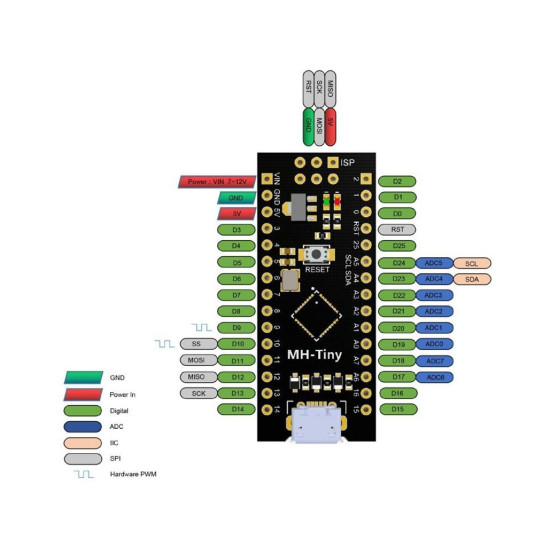
Despite its small footprint, the ATTiny88 provides access to 26 GPIO pins. Every pin features configurable internal pull-up resistors, digital input buffering, and software-configurable interrupt vectors. Dedicated internal timers drive hardware and software pulse-width modulation signals. Hardware PWM is mapped to pins D9 and D10 via Timer1 (a 16-bit timer/counter capable of precise phase-correct and fast PWM generation). Software-driven PWM routines can be instantiated across all 26 I/O pins via software interrupt service routines.
For analog data acquisition, the ATtiny88 features an 8-channel, 10-bit Analog-to-Digital Converter (ADC). The ADC channels allow developers to sample dynamic continuous voltages from analog temperature sensors, potentiometers, light-dependent resistors, and current sense shunts. Data bus communications are fully supported via high-speed SPI (Serial Peripheral Interface) and I2C / TWI (Two-Wire Interface), allowing the board to operate as a master or secondary peripheral device on shared sensor networks.
Detailed Pinout Assignments and Functional Map
Understanding the mapping of pins on the ATTiny88 is essential for hardware design and peripheral connection:
- VCC: 5V DC Regulated Output/Input Rail. Supplies regulated power to external sensors or receives 5V from an external regulated power supply.
- GND: Common Ground Reference Pins for power and logic communication.
- VIN: Unregulated DC Input Pin accepting 7V to 35V DC (12V max recommended). Feeds the onboard 500mA 5V LDO voltage regulator.
- D0 to D25 (26 GPIO Pins): Configurable General Purpose Digital Input/Output pins operating at 5V logic levels.
- D9 (PWM): Timer1 Channel A Output, providing hardware-based 16-bit high-resolution PWM output.
- D10 (PWM): Timer1 Channel B Output, providing hardware-based 16-bit high-resolution PWM output.
- A0 to A7 (ADC Pins): 10-bit Analog Input Channels multiplexed with digital GPIO pins (A0-A5 standard layout, A6-A7 extra analog lines).
- SDA / SCL (I2C): Hardware Two-Wire Interface pins for connecting I2C display modules, RTCs, and atmospheric sensor suites.
- MOSI / MISO / SCK / SS (SPI): Hardware Serial Peripheral Interface pins for high-speed synchronous communication with SD cards, wireless transceivers, and external memory chips.
- USB D+ / D-: Occupies two GPIO lines (typically pins D1 and D2) during active USB programming or V-USB HID communication. If USB communication is not actively utilized by user firmware, these lines can be reassigned as standard digital I/O pins.
Application Use Cases and Pinout Implementations
1. Low-Power Environmental Sensor Node
The ATTiny88 serves as an ideal edge node controller for remote microclimate monitor networks. An I2C atmospheric sensor (such as a BME280) is connected to the hardware SDA and SCL pins, while a capacitive soil moisture sensor outputs an analog signal to pin A0. The ATtiny88 samples data at dynamic intervals, executes threshold algorithms, and toggles an external LoRa RF transmitter via SPI (MOSI, MISO, SCK, SS). The low quiescent current of the board ensures prolonged operation when coupled with a battery source and a solar trickle charger on the VIN rail.
2. Custom Macro Keypad and USB HID Device
Leveraging the native V-USB stack supported by the Micronucleus bootloader, the ATTiny88 can be configured as a USB Human Interface Device (HID). Key switches arranged in a 3x3 matrix are connected to digital pins D3 through D11. When a key is actuated, the software debounce code processes the matrix state and transmits USB keyboard media shortcuts directly to a host PC via the onboard Micro-USB interface without requiring custom host-side driver installations.
3. Multi-Channel Software PWM LED Dimmer
By executing high-frequency software PWM routines using the internal 8-bit Timer0 interrupt, the ATTiny88 can control multi-channel LED lighting arrays. Pins D3 through D8 drive external N-Channel MOSFET gates connected to high-power LED strips. The board processes dynamic light patterns, dimming curves, and color blending commands received over an I2C serial link from a central controller board.
4. Miniature Battery-Operated Wearable Controller
Thanks to its ultra-compact 44.5mm x 18.3mm profile and negligible weight of 6 grams, this module easily integrates into smart garments and wearable electronics. Power is supplied via a single 3.7V LiPo battery stepped up to 5V or connected directly to the board logic. The microcontroller processes data from an onboard triple-axis accelerometer connected to pins A4 (SDA) and A5 (SCL) to trigger visual indicator patterns on addressable RGB LEDs wired to pin D3.
5. Smart I2C Secondary Controller for Complex Robotics
Main single-board computers often run short of real-time low-level real-time interrupt pins. The ATTiny88 can act as a dedicated peripheral co-processor. Connected to a primary Raspberry Pi or Arduino board via I2C (SDA/SCL), the ATTiny88 offloads real-time continuous pin monitoring, rotary encoder quadrature counting on pins D2 and D3, and limit switch debouncing across pins D4-D8, presenting cleaned data registers back to the main master controller on demand.
6. Programmable Pulse-Width Motor Speed Controller
Using the hardware Timer1 16-bit PWM generator on pins D9 and D10, the ATTiny88 generates high-precision, jitter-free PWM signals to drive dual DC motor H-bridge drivers (like the L298N or DRV8833). Analog input pin A0 reads control input from a 10k-ohm speed control potentiometer, while pins D4 and D5 set motor direction flags, producing precise control for small autonomous rover platforms.
7. Standalone Home Security Contact Node
In security automation, the board operates as a zero-latency magnetic reed switch monitor. Magnetic window/door contact switches are tied to digital pins D2 through D6 configured with internal pull-up resistors. When a contact loop breaks, a change-of-state interrupt wakes up the system, which triggers a piezo sounder on hardware pin D9 and updates a status bus line to a main home automation gateway.
8. Embedded High-Speed Frequency Meter and Data Logger
Utilizing internal hardware counter inputs, the ATTiny88 acts as a digital pulse counter for optical flow sensors or energy meters. Signal pulses enter pin D5 (External Clock Source input). Timer0 keeps track of precise clock intervals while Timer1 tallies incoming hardware pulses. Every second, calculated frequency metrics are logged to an external SPI Flash chip wired via SCK, MISO, MOSI, and SS pins for later extraction via USB.
Firmware Upload and Arduino IDE Integration
Programming the ATTiny88 via the Arduino IDE requires adding the ATTiny Core or MH-ET LIVE board support package manager URLs to your IDE preferences. Unlike typical boards that require selecting a COM port prior to uploading, the Micronucleus bootloader operates on a plug-and-verify basis: click Upload in the Arduino IDE, wait for the terminal to prompt user action, and then plug the ATTiny88 board into the USB port within 60 seconds. The bootloader detects the connection, writes the compiled binary file into the program Flash memory, verifies code integrity, and executes user code immediately.