





















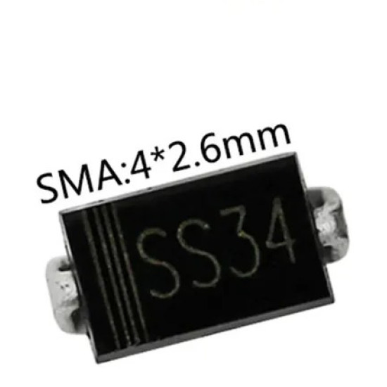


- Stock: In Stock
- Model: 1N5822 SMD Schottky Barrier Diode
- Weight: 0.05
- Dimensions: 7.90 x 5.90 x 2.30
- SKU: 4105
Architectural Overview and Semiconductor Physics
The 1N5822 surface-mount Schottky barrier rectifier diode represents a critical component in modern power electronics management, engineered specifically to deliver low-loss, high-efficiency current rectification in high-frequency switching environments. Unlike standard silicon PN-junction diodes that rely on minority carrier injection and subsequent recombination processes, the 1N5822 relies on a metal-to-semiconductor barrier junction. This physical architecture incorporates a proprietary metal barrier over an n-type epitaxial silicon layer, resulting in majority carrier conduction. This fundamental physics mechanism virtually eliminates minority carrier storage times, enabling near-instantaneous switching characteristics with zero reverse recovery time.
To mitigate the vulnerability of metal-semiconductor interfaces to high-voltage localized electric field concentration and thermal runaway, the 1N5822 integrates an advanced internal guard-ring structure. The guard-ring functions as a p-n junction perimeter network that acts as a stress-relief channel, distributing peak reverse voltage stress across a larger silicon area. This structural engineering enhances the diode dynamic voltage stress tolerance, minimizes localized reverse leakage current, and drastically improves long-term reliability in high-temperature operating conditions. Housed in a compact, low-profile SMC DO-214AB surface-mount package, the device maximizes power density by providing a high current carrying capacity of 3.0 Amperes while maintaining a thermal profile suitable for automated high-density board assemblies.
In-Depth Electrical Specifications and Thermal Performance
The electrical operating boundaries of the 1N5822 are tailored for low-voltage, high-frequency conversion systems. The component features a maximum repetitive peak reverse voltage rating of 40 Volts, a maximum RMS voltage of 28 Volts, and a maximum continuous DC blocking voltage of 40 Volts. Under continuous duty cycles, the device supports an average forward rectified current rating of 3.0 Amperes at a lead temperature of 95 degrees Celsius. When subjected to transient overload events, the internal junction architecture can sustain a non-repetitive peak forward surge current of up to 80 Amperes for an 8.3-millisecond single half-sine-wave pulse based on JEDEC method standards.
Thermal management and conduction efficiency are primary advantages of the 1N5822. The forward voltage drop is exceptionally low, measuring typically 0.475 Volts at a forward current of 3.0 Amperes with a junction temperature of 25 degrees Celsius, and dropping even lower under elevated thermal conditions. This low forward conduction voltage minimizes internal power dissipation calculated as forward voltage multiplied by forward current, resulting in directly reduced heat generation on the host printed circuit board. However, design engineers must account for the reverse leakage current profile, which measures approximately 0.5 milliamperes at rated DC blocking voltage at 25 degrees Celsius, increasing to 20 milliamperes at 100 degrees Celsius junction temperatures due to the inherent thermal excitation characteristics of Schottky barriers. Proper copper pad layout is essential to achieve typical junction-to-ambient thermal resistance values of 55 degrees Celsius per Watt or better.
Transient Response, High-Frequency Dynamics, and Switching Characteristics
In high-frequency power conversion applications, traditional silicon diodes experience substantial switching losses due to reverse recovery charge and reverse recovery time. The 1N5822 Schottky diode bypasses this limitation, exhibiting near-zero reverse recovery delay. When transitioning from forward conduction to reverse blocking state, the transient period is governed almost entirely by the charging of the internal junction capacitance, which is typically rated at 250 picofarads at a reverse voltage of 4.0 Volts and an operating test frequency of 1.0 Megahertz.
Because the switching speed is dictated by RC capacitive charging dynamics rather than carrier storage recombination, the device can operate seamlessly in high-frequency switching power supplies operating from 100 kilohertz up to several megahertz. The elevated switching speed dramatically reduces turn-off switching losses in the primary switching transistor, allowing for higher power conversion efficiency, smaller magnetic core components such as inductors and transformers, and smaller output filter capacitors. Additionally, the rapid response suppresses transient voltage spikes, minimizing electromagnetic interference generated during switching transitions.
Physical Package Dimensions, Mechanical Stresses, and Pinout Configuration
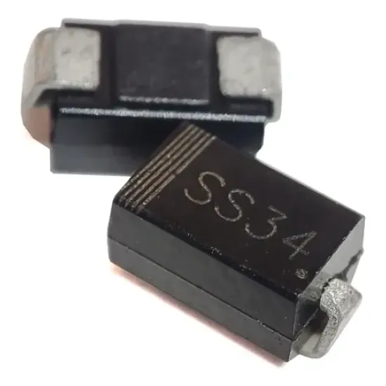
The 1N5822 surface-mount variant is encapsulated within a JEDEC DO-214AB SMC standard molded plastic package. The physical dimensions feature an overall package length of 7.95 mm inclusive of outer lead terminals, a body width of 5.85 mm, and a maximum body profile height of 2.25 mm. The package weight is approximately 0.21 grams. The outer leads are formed into a J-bend or flat lead configuration that reduces mechanical strain caused by thermal expansion coefficient mismatch between the epoxy glass PCB substrate and the device package mold compound.
The mechanical construction uses UL 94V-0 flame-retardant molding compound and meets moisture sensitivity level 1 standards per J-STD-020. The leads are tin-plated and fully solderable per MIL-STD-750 Method 2026, making the diode compatible with lead-free reflow soldering profiles with peak temperatures up to 260 degrees Celsius. The robust packaging allows high mechanical reliability against thermal cycling, mechanical shock, and vibration stresses typical in automotive, industrial, and high-reliability commercial electronics.
Pinout Identification and Terminal Layout
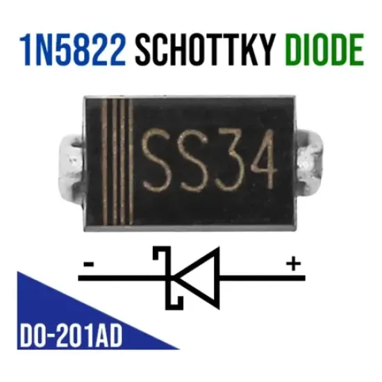
The 1N5822 surface-mount diode is a two-terminal polarized semiconductor device. Polarized identification is critical for correct circuit operation, as reverse installation will lead to short-circuit conditions or circuit failure.
Terminal 1 (Cathode): The cathode terminal is clearly designated on the physical body of the component by a distinct color band or recessed notch printed on the top surface of the molded plastic package. In standard circuit design, the cathode is connected to the more positive potential node during normal forward bias blocking or to the load node in rectification configurations.
Terminal 2 (Anode): The anode terminal is the unbanded end of the component package. Conventional current flows into the anode and out of the cathode when the forward voltage threshold of approximately 0.3V to 0.475V is exceeded.
Use-Cases and Implementation Engineering
1: High-Efficiency Buck DC-DC Converter Freewheeling Stage. In non-synchronous step-down buck converters, the 1N5822 serves as a freewheeling or catch diode connected across the switching node and system ground. When the high-side MOSFET turns off, the energy stored in the power inductor forces the switching node voltage below ground, forward-biasing the 1N5822. Current flows from ground through the diode and inductor to the load. The ultra-low forward voltage drop minimizes conduction losses during the off-time duty cycle, while the zero reverse recovery time prevents cross-conduction shoot-through spikes when the high-side switch turns back on, maximizing total converter efficiency.
2: Photovoltaic Module Hot-Spot Bypass Diode Protection. Solar panels consist of series-connected photovoltaic cells. When an individual cell is shaded or damaged, it ceases to generate power and becomes a high-resistance load, causing current from adjacent unshaded cells to force reverse voltage across it, leading to localized heating hot-spots and permanent damage. Connecting the 1N5822 in parallel anti-parallel orientation across groups of solar cells provides a bypass path. When shading occurs, the bypass diode becomes forward-biased, routing current safely around the shaded segment. The low thermal resistance and 3A rating allow continuous bypass operation in outdoor high-ambient environments.
3: Battery-Powered Reverse Polarity Protection. Electronic devices powered by removable batteries or external DC power adapters require protection against inverted battery insertion or wrong-polarity wiring. Placing the 1N5822 in series with the positive DC input rail ensures that current only flows when correct polarity is applied. Due to the ultra-low 0.475V forward drop of the Schottky barrier compared to a standard 0.7V to 1.0V silicon diode, voltage headroom is preserved, extending usable battery life and reducing thermal dissipation within sealed handheld enclosures.
4: Asynchronous Boost Converter Output Rectification. In boost DC-DC topologies, the 1N5822 functions as the output energy transfer element positioned between the inductor switching node and the output storage capacitor. When the boost switch turns off, the inductor voltage rises above the input rail, forward-biasing the diode and transferring energy to the output capacitor. The low junction capacitance of 250 pF and rapid response time prevent high-frequency ringing and minimize output ripple, enabling smooth voltage step-up for LED drivers, sensor nodes, and communication modules.
5: Diode OR-ing Logic for Redundant DC Power Bus Networks. Mission-critical electronics often rely on multiple power sources, such as a main AC-DC wall supply and an internal backup battery rail. Integrating two 1N5822 diodes in a common-cathode OR-ing configuration allows seamless automatic power supply transition. The load is powered by whichever source provides the higher voltage level. The low reverse leakage current prevents cross-charging between supplies, while low forward drop maximizes system power delivery efficiency without requiring complex active MOSFET controllers.
6: High-Speed Flyback Clamp in Solenoid and Relay Inductive Drivers. Driving inductive loads such as electromechanical relays, solenoids, and DC motors with transistors creates severe inductive voltage spikes upon switch turn-off. Placing the 1N5822 in anti-parallel across the inductive coil provides a safe circulation path for the collapsing magnetic field energy. The ultra-fast switching speed captures the sharp transient immediately, protecting sensitive driving MOSFETs or bipolar transistors from avalanche breakdown.
7: Secondary-Side Output Rectification in Isolated Flyback Converters. In isolated switch-mode power supplies, high-frequency transformers step down primary high voltages to low output rails such as 3.3V, 5V, or 12V. The 1N5822 is configured on the secondary winding output stage to rectify high-frequency 100kHz to 500kHz AC pulses into smooth DC current. Its high current rating of 3A and low forward power loss make it ideal for secondary regulation in wall adapters, router power supplies, and industrial controllers.
8: Energy Harvesting Ultralow-Loss Micro-Power Isolation. Energy harvesting systems utilizing piezoelectric, thermoelectric, or small solar cells yield tiny quantities of electrical power. The 1N5822 is utilized in bridge or blocking configurations to isolate storage supercapacitors or thin-film batteries from harvesting transducers. Its exceptionally low forward turn-on threshold ensures maximum energy capture from minimal ambient energy excitation.
PCB Surface Mount Design Guidelines, Thermal Sinking, and Reflow Profiles
To ensure optimal thermal dissipation and high current reliability when deploying the 1N5822 in SMC packaging, layout engineers must adhere to thermal land pattern recommendations. Copper pads should extend beyond the lead footprint by at least 1.5 mm to serve as localized heat sinks. Utilizing multi-layer ground planes connected via thermal vias under the cathode pad substantially reduces junction-to-ambient thermal resistance, preventing thermal runaway caused by reverse leakage current at elevated temperatures.
During assembly, automated surface-mount technology pick-and-place equipment accurately positions the component on solder paste stencils with typical thickness between 0.127 mm and 0.152 mm. Reflow profiles should follow J-STD-020 standards, maintaining a preheat ramp rate of 1 to 3 degrees C per second, a soak time of 60 to 120 seconds between 150 and 200 degrees C, and a peak reflow temperature of 245 to 260 degrees C for no longer than 30 seconds. Compliance with these parameters ensures sound solder joint formation without inducing thermal shock to the internal Schottky barrier metal junction.