


















- Stock: In Stock
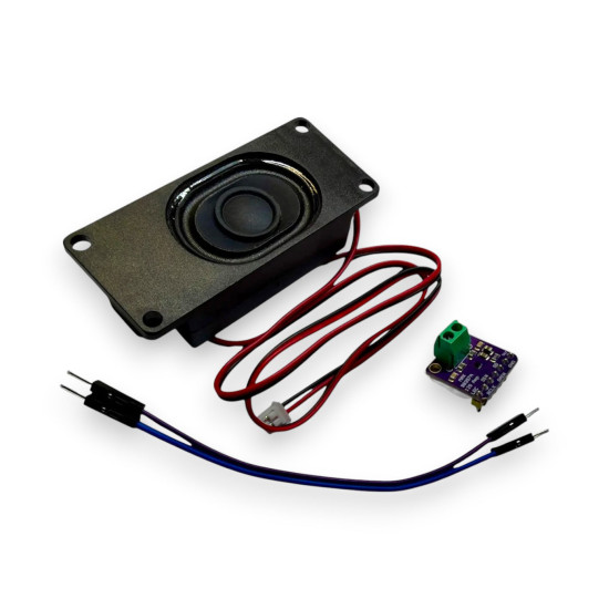
- Model: MAX98357A I2S Class-D Audio Am
- Weight: 2.50
- Dimensions: 19.00 x 18.00 x 3.20
- SKU: 4106

Comprehensive Technical Overview
The MAX98357A I2S Class-D Audio Amplifier Breakout Board represents a sophisticated, highly integrated digital audio playback solution tailored for modern embedded systems, microcontrollers, and single-board computers (SBCs). Unlike traditional analog audio power amplifiers that demand an external Digital-to-Analog Converter (DAC) or analog PWM modulation hardware, the MAX98357A interfaces directly with pure digital audio data streams over the standard I2S (Inter-IC Sound) serial protocol. By combining a high-precision pulse-density modulation (PDM) DAC stage and an ultra-efficient Class-D audio output driver into a single compact silicon die, this module eliminates noise induction along analog traces, drastically reduces component count, and maximizes electrical efficiency for power-constrained implementations.
Capable of delivering up to 3.2 watts of continuous RF-filtered power into a 4-ohm load at a 5V supply, or 1.4W into an 8-ohm load at 3.7V lithium-ion battery voltages, the MAX98357A delivers rich, high-fidelity sound with minimal thermal dissipation. The circuit automatically decodes standard pulse-code modulation (PCM) data at sample frequencies ranging from 8kHz up to 96kHz, making it versatile enough for low-bitrate voice annunciators as well as high-definition audio playback applications. Crucially, the MAX98357A incorporates an integrated phase-locked loop (PLL) that synthesizes the internal master clock (MCLK) directly from the incoming bit clock (BCLK), freeing hardware designers from routing an additional high-frequency master clock line across system boards.
Silicon Architecture and Internal Operation
At the core of the MAX98357A architecture is a high-performance filterless Class-D power amplifier topology utilizing active edge-rate limiting and spread-spectrum modulation scheme. Traditional Class-D amplifiers require bulky LC output filters to attenuate the high-frequency switching waveform and prevent high electromagnetic interference (EMI). The MAX98357A solves this problem using patented edge-rate control and active modulation techniques that minimize high-frequency switching noise while maintaining efficiency above 92%. The differential output drive topology (Bridge-Tied Load or BTL) drives speaker coils directly using balanced outputs, doubling the effective voltage swing across the speaker load without requiring a high supply rail or DC blocking capacitors.
The module dynamic range exceeds 92dB with an exceptionally low Total Harmonic Distortion plus Noise (THD+N) rating of just 0.015% at 1kHz/1W into an 8-ohm load. Additionally, integrated click-and-pop suppression logic monitors supply rails and digital clock signals during power-up and power-down transitions, suppressing audible transients completely during turn-on and turn-off phases. The chip features thermal overload protection, short-circuit protection, and undershoot limiters to prevent physical silicon failure under harsh reactive speaker loads.
Pinout Architecture and Interface Signal Breakdown
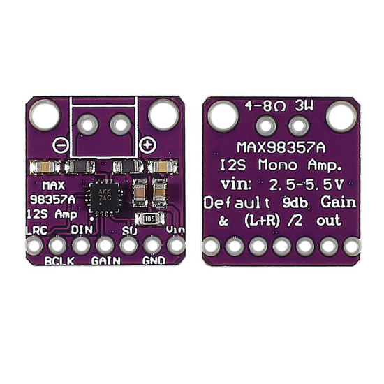
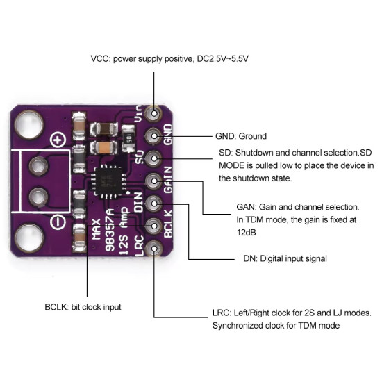
The module exposes eight standard 2.54mm (0.1 inch) header pads designed for breadboard prototyping or wire connections, along with two screw-terminal pads or direct wire solder points for speaker lines. Below is the detailed breakdown of every pin interface:
- VIN (Power Input): System positive power rail supplying operating voltage directly to the IC and switching bridge. Accepts input DC voltages from 2.5V to 5.5V. Must be decoupled with a 10uF ceramic capacitor placed adjacent to the board.
- GND (Ground): Common reference ground plane for both digital signals and high-current power return. Ensure low-impedance connection to the host board ground.
- SD_MODE (Shutdown and Channel Selection): Multi-function digital input pin used to disable the IC into sub-microamp mode or configure audio channel decoding (Left, Right, or Mixed Mono). A logic low (<0.16V) powers down the internal circuitry.
- GAIN (Gain Setting Input): Analog/Digital configuration pin used to program internal gain levels between 3dB and 15dB. Floating or connecting via specific resistors to GND or VIN selects distinct gain factors.
- DIN (Digital Data Input): Serial data pin receiving standard I2S or Left-Justified PCM audio stream data bits synchronized to BCLK.
- BCLK (Bit Clock Input): High-speed clock input driving digital serial data shifted into the DIN register. Frequency is typically 32 or 64 times the sample rate.
- LRC (Left/Right Frame Sync Clock Input): Low-frequency clock input defining the start of each audio frame and indicating whether data belongs to the left or right channel (typically equal to the sample rate, e.g., 44.1kHz or 48kHz).
- OUT+ and OUT- (Differential Output): Class-D Bridge-Tied Load (BTL) speaker output channels. Connect directly across passive speaker terminals (4 ohm to 8 ohm). Do not ground either terminal.
Comprehensive Gain and Shutdown Configuration Guide
The GAIN pin enables hardware configuration of system gain without requiring software modifications or firmware overhead. By setting the voltage level on the GAIN input, five distinct amplification factors are available:
- 15dB Gain: Connect GAIN pin to GND through a 100k ohm resistor. Recommended for low-level digital signals or low supply voltages.
- 12dB Gain: Connect GAIN pin directly to GND (0V). Ideal standard default gain for typical 3.3V host interfaces.
- 9dB Gain: Leave GAIN pin Floating / Unconnected. Default mode when no pin header connection is made.
- 6dB Gain: Connect GAIN pin directly to VIN. Optimized for high digital amplitude signals to prevent speaker clipping.
- 3dB Gain: Connect GAIN pin to VIN through a 100k ohm resistor. Provides maximum headroom for maximum supply rail operation.
The SD_MODE pin provides flexible operational states depending on the voltage applied to it relative to VIN. When pulled below 0.16V, the chip enters a low-power shutdown state drawing less than 1 microamp. When pulled high, internal voltage comparators decode the pin voltage to choose audio channel extraction:
- Left Channel Mode: Pulled high to VIN via a pull-up resistor (>100k ohm) or directly driven high. Decodes audio data from the Left I2S time slot.
- Right Channel Mode: Pulled high to VIN via a series resistor setting the pin voltage between 0.7V and 1.4V. Decodes audio data from the Right I2S time slot.
- Stereo Mix / Mono Mode: Left floating or pulled to an intermediate voltage (~0.4V to 0.6V). Automatically averages Left and Right channel sample data into a balanced single mono stream.
Hardware Application Use-Cases
1. ESP32 Wi-Fi Internet Radio Streamer: Combined with an ESP32 microcontroller, the MAX98357A forms a minimalist internet radio receiver. The ESP32 fetches MP3 or AAC streams over Wi-Fi, decodes them via software libraries, and outputs pure raw PCM over I2S pins (BCLK, LRC, DIN) directly into the module to drive desktop speakers without an external DAC shield.
2. Raspberry Pi Retro Gaming Console Audio Engine: Ideal for compact handheld gaming consoles based on Raspberry Pi Zero or Raspberry Pi 4. By outputting digital sound over the Pi GPIO I2S bus (GPIO18, GPIO19, GPIO21), the MAX98357A delivers crystal-clear 8-bit chip-tune and 16-bit sound effects directly to miniature arcade speakers, completely avoiding noisy analog PWM jack outputs.
3. Custom Smart Assistant and Voice UI Endpoint: In custom voice-controlled hardware powered by platforms like Home Assistant, local voice models trigger speech playback responses. The MAX98357A delivers immediate speech response notifications with zero background hiss or ground loop hum, critical for clean ambient audio in home automation units.
4. Industrial IoT Safety Annunciator and Voice Alerting: Implemented within factory automation equipment and alarm panels, the board translates flash memory audio alerts into high-decibel speech notifications. The robust 3.2W drive strength allows industrial equipment to sound audible alerts across noisy machine shop floors.
5. STM32 Modular Synthesizer and Waveform Generator: Electronic music instruments utilizing STM32 microcontrollers synthesize complex audio waveforms via direct memory access (DMA) to the I2S peripheral. The MAX98357A receives 16-bit or 24-bit audio streams directly, driving synthesizer line outputs or small monitoring speakers with high dynamic range.
6. Autonomous Mobile Robot Audio Interface: Mobile robots rely on clear audio cues for human interaction and status feedback. The power efficiency of the Class-D topology preserves precious lithium battery energy while delivering clear diagnostic prompts, system error chimes, and proximity warnings.
7. Bluetooth Audio Receiver Node with ESP32-A2DP: Pairing the module with the ESP32 Bluetooth A2DP audio sink profile allows makers to create custom wireless speakers. Digital Bluetooth audio packets are streamed straight to the MAX98357A over digital lines, guaranteeing optimal signal-to-noise performance.
8. Interactive Museum Exhibit and Kiosk Display Output: Built into interactive touchscreens, smart vending machines, and educational museum kiosks, the module provides reliable sound effects during user interactions. Automatic power control via SD_MODE ensures silent operation during idle exhibit states without electrical pop noises during awakenings.
Hardware Integration, Layout and PCB Guidelines
To ensure maximum acoustic performance and prevent high-frequency noise interference, proper PCB layout techniques must be observed when integrating the MAX98357A module. Keep digital I2S trace lengths (BCLK, LRC, DIN) as short and matched in length as possible to minimize jitter and signal radiation. Route speaker traces from OUT+ and OUT- as a parallel differential pair directly to the speaker terminal. If speaker wire runs exceed 20 centimeters, place ferrite beads (100 ohm at 100MHz) in series with OUT+ and OUT- adjacent to the board to maintain strict FCC radiated emissions compliance.