Top Seller
Out Of Stock


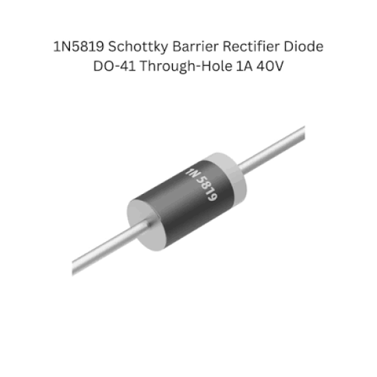
1N5819 SCHOTTKY BARRIER DIODE 1A 40V
KES 5.00
- Stock: Out Of Stock
- Model: 1N5819
- Weight: 0.33g
- Dimensions: 5.20mm x 2.70mm x 2.70mm
- SKU: 724
This product has a minimum quantity of 5
Your shopping cart is empty!


The 1N5819 is an industry-standard, axial-leaded Schottky barrier rectifier diode engineered specifically for high-efficiency, high-frequency electronic switching applications and low-voltage power distribution networks. Unlike standard silicon PN junction diodes that rely on minority carrier injection and recombination, the 1N5819 operates via a metal-to-semiconductor barrier interface, utilizing a platinum or chrome barrier metal deposited on an N-type silicon substrate. This fundamental physical architecture classifies the device as a majority-carrier conduction device, entirely eliminating the minority-carrier storage time that plagues conventional PN rectifiers like the 1N400x family. Consequently, the 1N5819 exhibits near-instantaneous switching behavior, negligible reverse recovery time, and an exceptionally low forward voltage drop, establishing it as a foundational component for hardware designers striving to minimize conduction and switching losses in low-voltage circuitry.
At the center of the 1N5819 performance matrix is its Schottky barrier interface. In a standard PN junction, forward bias forces electrons and holes across the depletion boundary, requiring a finite duration for charge clearance when reverse bias is applied, commonly termed reverse recovery time. In the 1N5819, conduction occurs strictly through thermionic emission of majority carrier electrons over the potential barrier formed between the metal anode contact and the epitaxial semiconductor lattice. Because no charge storage mechanism exists in the depletion region, reverse recovery transients are theoretically limited only by the intrinsic parasitic junction capacitance and small series package inductances. In practical terms, this allows the diode to transition between conduction and blocking states at frequencies extending well into the hundreds of kilohertz and low megahertz spectrum without substantial dynamic switching power dissipation.
The forward conduction curve of the 1N5819 delivers an exceptionally low forward voltage drop (VF) under standard operating regimes. While a standard silicon rectifier typically drops between 0.7V and 1.1V under forward bias, the 1N5819 maintains an ultra-low threshold, measuring approximately 0.36V to 0.45V at low to moderate current levels, and peaking at roughly 0.60V under its maximum continuous forward current rating of 1.0 Ampere at 25 degrees Celsius. Because power dissipation within the silicon die is directly proportional to forward current multiplied by forward voltage (P = IF x VF), the 1N5819 cuts steady-state thermal dissipation by up to 50 percent relative to traditional rectifiers. However, circuit designers must balance this low forward drop against the intrinsic trade-off of Schottky barrier devices: increased reverse leakage current (IR). At maximum rated reverse voltage (40V DC) and room temperature, reverse leakage remains within tens of microamperes, but this value increases exponentially at elevated junction temperatures, mandating careful thermal budgeting to prevent thermal runaway conditions.
The operational limits of the 1N5819 are precisely characterized across continuous and transient electrical regimes. The repetitive peak reverse voltage (VRRM), working peak reverse voltage (VRWM), and continuous DC blocking voltage (VR) are rated at a maximum of 40 Volts. This voltage ceiling makes the device optimized for secondary rectification in 5V, 12V, and 24V distributed power systems, while offering an adequate safety margin against transient voltage overshoots. The average forward rectified current (IF(AV)) is specified at 1.0 Ampere continuous under an ambient temperature threshold of 90 degrees Celsius, using standard 0.375-inch lead lengths tied to appropriate printed circuit board copper traces. When subjected to transient surges, the non-repetitive peak forward surge current (IFSM) withstands up to 25 Amperes for an 8.3 millisecond single half-sine wave under rated load conditions, providing robust survival margins against inrush currents caused by bulk capacitive bank charging during power initialization.
Dynamic parasitic characteristics include a typical junction capacitance (CJ) of approximately 110 picofarads measured at 1.0 megahertz with a reverse voltage bias of 4.0 Volts. The thermal resistance from junction to ambient (R-theta-JA) is approximately 80 degrees Celsius per Watt when mounted on standard FR4 laminates, while junction-to-lead resistance (R-theta-JL) measures roughly 28 to 30 degrees Celsius per Watt. The diode is certified for operation across an extended junction operating and storage temperature envelope spanning from minus 65 degrees Celsius to plus 125 degrees Celsius, allowing deployment in demanding commercial, industrial, and automotive peripheral environments.
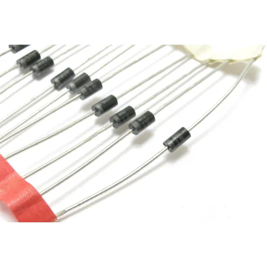
The 1N5819 is encapsulated within the globally recognized, hermetically sealed JEDEC DO-41 (also known as DO-204AL) axial leaded package. The physical envelope features a molded plastic body engineered with UL 94V-0 flame-retardant epoxy, ensuring superior thermal transfer and environmental passivity against moisture ingress. The axial leads are composed of high-purity, tin-plated copper with excellent solderability, adhering to MIL-STD-202 specifications. The overall package body length spans approximately 4.10 to 5.20 millimeters with an outer diameter between 2.00 and 2.70 millimeters. The lead wire diameter measures standard 0.71 to 0.86 millimeters, providing high structural rigidity and minimal lead resistance.
The physical pinout follows standard diode polarities: it is a two-terminal component consisting of an Anode and a Cathode. Polarity orientation is visually indicated by a prominent laser-etched or silkscreened cathode band located at one end of the DO-41 body. Current flows conventionally from the unbanded lead (Anode) to the banded lead (Cathode) under forward bias conditions. In high-vibration applications, the axial leads can be bent and stress-relieved using standardized forming tools, ensuring minimum lead-bend radiuses to prevent micro-fracturing of the glass-to-metal internal die passivation layer.
1. High-Efficiency Buck Regulator Freewheeling (Catch) Diode: In non-synchronous step-down DC-DC switching converters operating up to several hundred kilohertz, the 1N5819 functions as the essential freewheeling diode. Positioned across the switching node and system ground, it provides a low-impedance circulating current path for inductor energy during the main transistor turn-off interval. The ultra-low forward voltage drop minimizes duty-cycle energy loss, significantly boosting converter efficiency in 12V-to-5V or 5V-to-3.3V power rails.
2. Reverse Battery and Power Polarity Protection: Battery-powered embedded systems, handheld instruments, and field devices are susceptible to permanent failure caused by inverted battery insertion or reverse DC jack connections. Placing a 1N5819 in series with the positive input rail blocks destructive reverse currents up to 40V. Its minimal forward conduction loss ensures low battery voltage drops, extending battery operating lifespan compared to standard silicon diodes.
3. Solar Cell Array Bypass and Blocking Elements: In low-power photovoltaic panels and micro-harvesting solar modules, the 1N5819 serves both as a reverse blocking diode to prevent battery drainage through dark panels during nighttime, and as a bypass diode parallel to strings of solar cells. Its low threshold voltage avoids wasting valuable millivolts generated by low-irradiance solar cells, maximizing overall energy harvesting yield.
4. Inductive Kickback Snubbing for Relays and Solenoids: Driving electromechanical coils, relays, miniature DC motors, and solenoids with microcontrollers and low-side MOSFETs generates high-voltage inductive flyback spikes upon de-energization (V = -L di/dt). Placing a 1N5819 anti-parallel to the inductive coil safely clamps transient spikes to roughly 0.5V above the positive rail, protecting sensitive driver transistors from avalanche breakdown.
5. Dual-Supply OR-ing and Uninterruptible Power Supply (UPS) Multiplexing: Devices powered concurrently by USB (5V) and an auxiliary battery (4.2V lithium-ion) rely on Schottky OR-ing diode networks to seamlessly transition between primary and secondary power sources without backfeeding. The 1N5819 provides ideal low-loss steering, ensuring the higher voltage supply powers the load while preventing reverse conduction into the lower-voltage cell.
6. Switched-Mode Flyback Secondary Output Rectifier: In low-wattage isolated flyback converters, such as wall adapters and auxiliary microcontroller biases, the 1N5819 rectifies high-frequency AC waveforms delivered across the secondary transformer winding. The virtually instantaneous reverse recovery eliminates severe ringing and high-frequency EMI, drastically simplifying output filter design and snubber network complexity.
7. High-Speed Logic Rail Clamping and Overvoltage Protection: Sensitive analog-to-digital converter (ADC) inputs, I2C lines, and microcontroller GPIO pins are vulnerable to external overvoltage transients and signal overshoot. A pair of 1N5819 diodes arranged in a rail-to-rail clamping configuration steers positive and negative transient overshoots safely into the supply rails before internal silicon ESD structures are damaged.
8. Charge-Pump Voltage Doubler and Inverter Circuits: Switched-capacitor charge pumps rely on sequential diode conduction to shuttle charge between reservoir capacitors to double, triple, or invert voltages. Because charge pump output impedance is strongly dictated by diode forward voltage drops, the low VF of the 1N5819 guarantees minimal voltage drops, achieving maximum voltage transfer efficiency in analog level-shifting networks.
Effective thermal management is vital when implementing the 1N5819 in continuous 1 Ampere circuits. Although the DO-41 package is compact, heat generation must be dissipated through its axial leads into the circuit board copper planes. Designers should maximize copper pad surface area at both the anode and cathode landing pads, utilizing 2-ounce copper when possible to lower the overall thermal resistance from junction to ambient. Because Schottky diodes feature high reverse leakage currents at elevated operating temperatures, inadequate board heat sinking can lead to an unstable thermal runaway loop: higher temperatures cause elevated leakage current, which generates higher internal self-heating, ultimately causing device breakdown. Lead lengths should be trimmed as short as practically feasible (standard 4mm to 6mm) to facilitate optimal heat conduction away from the molded package body into the supporting printed circuit board tracks.
Ginō AI - Nerokas AI Assistant