


- Stock: In Stock
- Model: 74LS93
- SKU: 3615
The 74LS93 is a 4-bit binary counter made of two up-counters. The IC consists of a mode-2 up-counter and a mod-8 up counter. Can be combined as mod-8 counter or divide by 2 or divide by 8 applications. It is built using four JK Flip Flops.
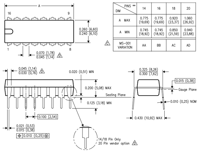
Pin Description
Pin Number | Pin Name | Description |
1,2,3,6 | NC | No Connection |
4,5,8,9 | Q0, Q1, Q2, Q3 | Output pins |
7 | Ground | Connected to ground of the system |
10 | CP0 | Clock Input – divide by 2 |
11 | CP1 | Clock Input – divide by 8 |
12,13 | MR | Master Reset – Clear Input |
14 | Vcc | Supply voltage – 4.5V to 5.5V |
Features
- 4-Bit Binary Counter IC
- Typical Operating Voltage: 5V
- Operating Voltage Range: 4.5V to 5.5V
- Output High Voltage: 3.5V
- Output Low Voltage: 0.25V
- Output current when high: -0.4mA
- Output current when low: 8mA
- CP0 and CP1 input clock frequency: 32MHz and 16MHz resp.
- CP0 and CP1 pulse width: 15nS and 30nS resp.
- Available in 14-pin PDIP, GDIP, PDSO packages
74LS93 Equivalents
74HC19, 74LS192, 4516
Other Counter ICs
74LS90, CD4017, 74LS02, CD4020, CD4060, CD4022
Where to use 74LS93?
The 74LS93 is a up-counter built using four JK flip-flops. The CP1 and Q0 forms a mod-2 counter using a single flip-flop and the CP0 with Q1, Q2 and Q3 with three flip-flops forms the mod-8 counter. The IC is commonly used by combining mod-2 and mod-8 to form a mod-16 up-counter. The IC is commonly used in counting applications or in divide by 2, divide by 8 or divide by 16 designs.
How to use 74LS93
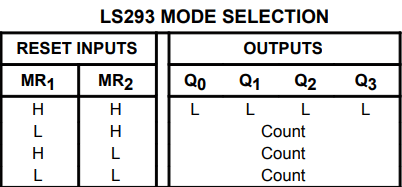
Using the 74LS93 IC is easy and straight forward. The IC has to be powered by Vcc and ground pin using +5V. It has two MR (Master reset) pin which can be used to select the required mode. For normal operation both the pins has to be connected to ground (LOW) as mentioned in the table below.
Next for the clock pin CP0 and CP1 we have to provide a clock pulse for the counting to happen. That is the IC will increase the count by 1 for every pulse given to these clock pins. The output bit Q0 is controlled by CP1 and output bits Q1,Q2 and Q3 is controlled by CP0. To use all four bits the clock pulse CP1 is connected to Q0.
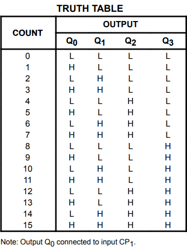
The maximum clock frequency for CP0 and CP1 can be 32MHz and 16MHZ respectively and the pulse width should be minimum of 15nS and 30nS respectively. Normally the clock pin is driven by a 555 timer or other pulse generating circuits. The output bits getting incremented in shown in table below.
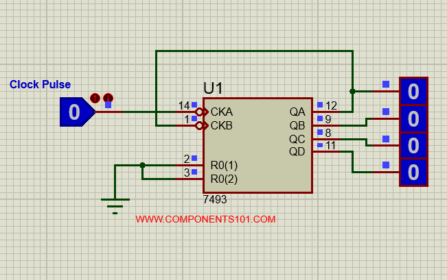
The complete working can be understood by simulating the IC. Here mode-0 (counting mode) is selected by grounding both MR pins and for the clock pulse I am manually toggling a logic state to provide pulse. Every time I make the pin high and low a single pulse is generated. The simulation is shown below
Further, you can also watch the video below for a complete understanding of the IC.
Applications
- Used for creating long timing period
- Astable frequency divider or counter circuit
- Timing related applications
- Used in project where Microcontrollers should be avoided
- Pulse counter or frequency divider
2D-Model